Fast recovery epitaxial diode and preparation method thereof

A diode and epitaxy technology, which is applied in semiconductor/solid-state device manufacturing, electrical components, circuits, etc., can solve the problems of long process flow, long production cycle, and many manufacturing processes, so as to shorten the process flow, improve ohmic contact, and reduce environmental pollution. pollution effect

Inactive Publication Date: 2012-06-13
MACMIC SCIENCE & TECHNOLOGY CO LTD
View PDF6 Cites 19 Cited by
  • Summary
  • Abstract
  • Description
  • Claims
  • Application Information

AI Technical Summary

Problems solved by technology

[0003] At present, the preparation methods of epitaxial fast recovery diodes (FRED) all use N-type epitaxial silicon wafers as materials, and the P-type active region is realized by ion implantation or boron diffusion. Active area engraving, ion implantation, junction pushing, photolithography electrode hole, metallization, photolithography metal, deposition passivation layer, photolithography passivation layer, silicon wafer thinning, back metallization process, in the production process, Multiple ion implantation, high-temperature push junction and at least four photolithography are required, not only complicated operation, many manufacturing processes, long process flow, but also long production cycle, resulting in high manufacturing cost and poor market competitiveness

Method used


Image

  • Fast recovery epitaxial diode and preparation method thereof
  • Fast recovery epitaxial diode and preparation method thereof

Examples


Embodiment Construction

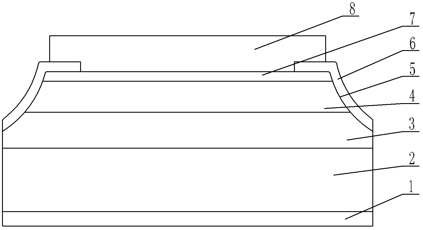
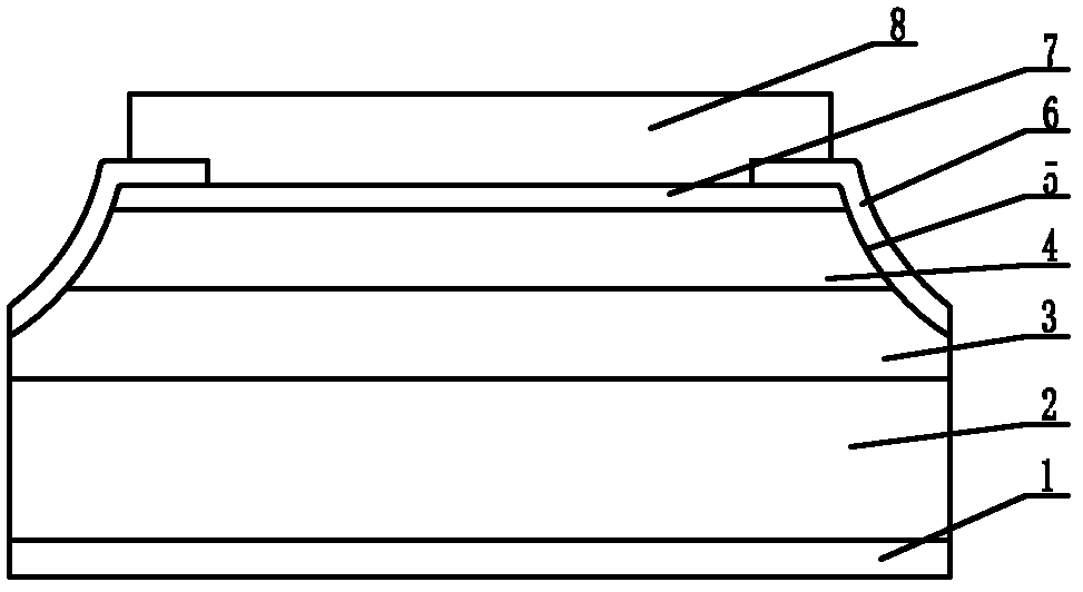
[0025] The preparation method of fast recovery epitaxial diode of the present invention, according to the following steps:

[0026] (1) Growth of the first epitaxial layer: grow more than one layer of N-type first epitaxial layer on the front side of the N+ type substrate silicon wafer, the total thickness of which is controlled at 1-300 μm, and the resistivity is 1-150 ohm cm. The thickness of the first N-type epitaxial layer can be controlled at 30-200 μm, and the resistivity is 20-100 ohm centimeters. The N-type epitaxial layer can be grown once, twice or three times, so that the N+ type substrate grown on the front side of the silicon wafer Type of the first epitaxial layer as a drift region.

[0027] (2) Growth of the second epitaxial layer: grow a layer of P-type second epitaxial layer on the first epitaxial layer, its thickness is controlled at 1-30 μm, and the impurity concentration is controlled at 10 13 ~10 18 cm -3 , the thickness can also be controlled at 5-18 μ...


PUM

PropertyMeasurementUnit
thicknessaaaaaaaaaa
thicknessaaaaaaaaaa
thicknessaaaaaaaaaa

Abstract

The invention relates to a fast recovery epitaxial diode comprising a metal cathode layer, an N + substrate silicon chip, a first epitaxial layer, a second epitaxial layer, a third epitaxial layer, wherein the above-mentioned parts are successively connected. A mesa silicon groove penetrates the third epitaxial layer and is extended into the second epitaxial layer; a glass passivation layer that is arranged inside the mesa silicon groove and is provided with a window is extended to the top surface of the third epitaxial layer; and a metal anode layer that is arranged at the upper portion of the glass passivation layer passes through the window that is arranged on the glass passivation layer and then is connected with the third epitaxial layer. According to the invention, an epitaxial technology is used to accurately control impurity concentration and thickness of all the epitaxial layers; and a mesa channeling technology and a glass passiviation technology are utilized to manufacture a terminal structure, thereby substantially reducing a technology flow. Besides, the fast recovery epitaxial diode has good consistency and repeatability; high quality characteristics including low forward direction voltage drop, super speediness, and soft recovery characteristic and the like of the fast recovery epitaxial diode can be easily realized.

Description

technical field [0001] The invention relates to a fast recovery epitaxial diode and a preparation method thereof, belonging to the technical field of semiconductor devices. Background technique [0002] As a new generation of new power semiconductor devices, FRED has the advantages of high frequency, high voltage, high current, low loss and low electromagnetic interference. Together with IGBT, it is recognized by the international power electronics industry as the most representative of the third revolution of power electronics technology. device. FRED can be used alone as a PFC diode, output rectifier diode, clamping diode, and absorbing diode, or as a freewheeling diode and used in conjunction with IGBT. FRED single tube and module and combined with IGBT are widely used in motor speed regulation, such as : Washing machines, air conditioners, refrigerators, electric vehicles, urban rail transit, locomotive traction, various fans, water pumps and wind and solar power genera...

Claims


Application Information

Patent Timeline
Patent Type & Authority Applications(China)
IPC IPC(8): H01L21/329H01L21/28H01L29/861H01L29/45
Inventor 刘利峰张景超吴迪林茂戚丽娜
Owner MACMIC SCIENCE & TECHNOLOGY CO LTD
Why Eureka
Try Eureka