Process for manufacturing gallium nitride-base GaN power integrated circuit

An integrated circuit, gallium nitride-based technology, applied in circuits, semiconductor/solid-state device manufacturing, electrical components, etc., can solve the problems of general electronic circuit system design incompatibility, increase system power consumption and volume, and shorten the drift zone length, reducing the surface electric field, reducing the effect of additional stress

An integrated circuit, gallium nitride-based technology, applied in circuits, semiconductor/solid-state device manufacturing, electrical components, etc., can solve the problems of general electronic circuit system design incompatibility, increase system power consumption and volume, and shorten the drift zone length, reducing the surface electric field, reducing the effect of additional stress

CN102543871AInactive Publication Date: 2012-07-04WUXI JINGKAI TECH

Image

  • Process for manufacturing gallium nitride-base GaN power integrated circuit
  • Process for manufacturing gallium nitride-base GaN power integrated circuit
  • Process for manufacturing gallium nitride-base GaN power integrated circuit

Examples


Embodiment Construction

[0039] The GaN gallium nitride-based process development and boost chip design involved in the present invention will be further described below in conjunction with the accompanying drawings and examples.

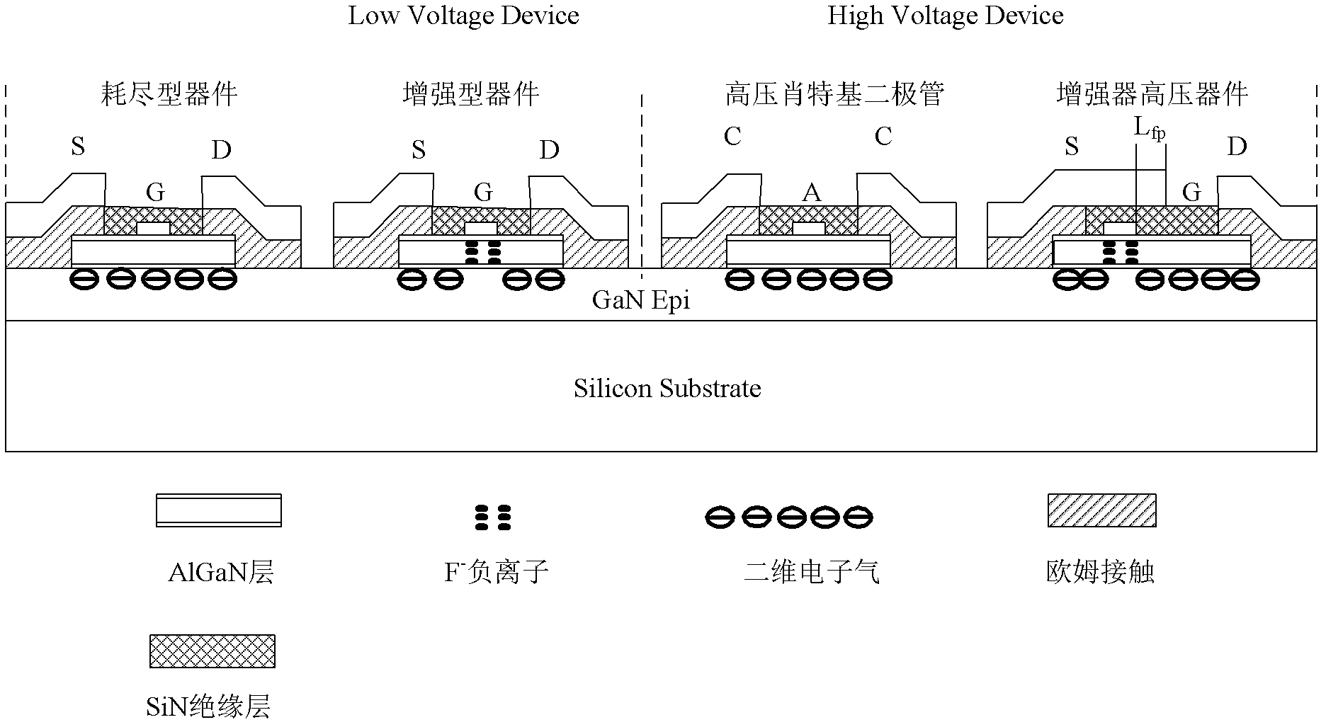
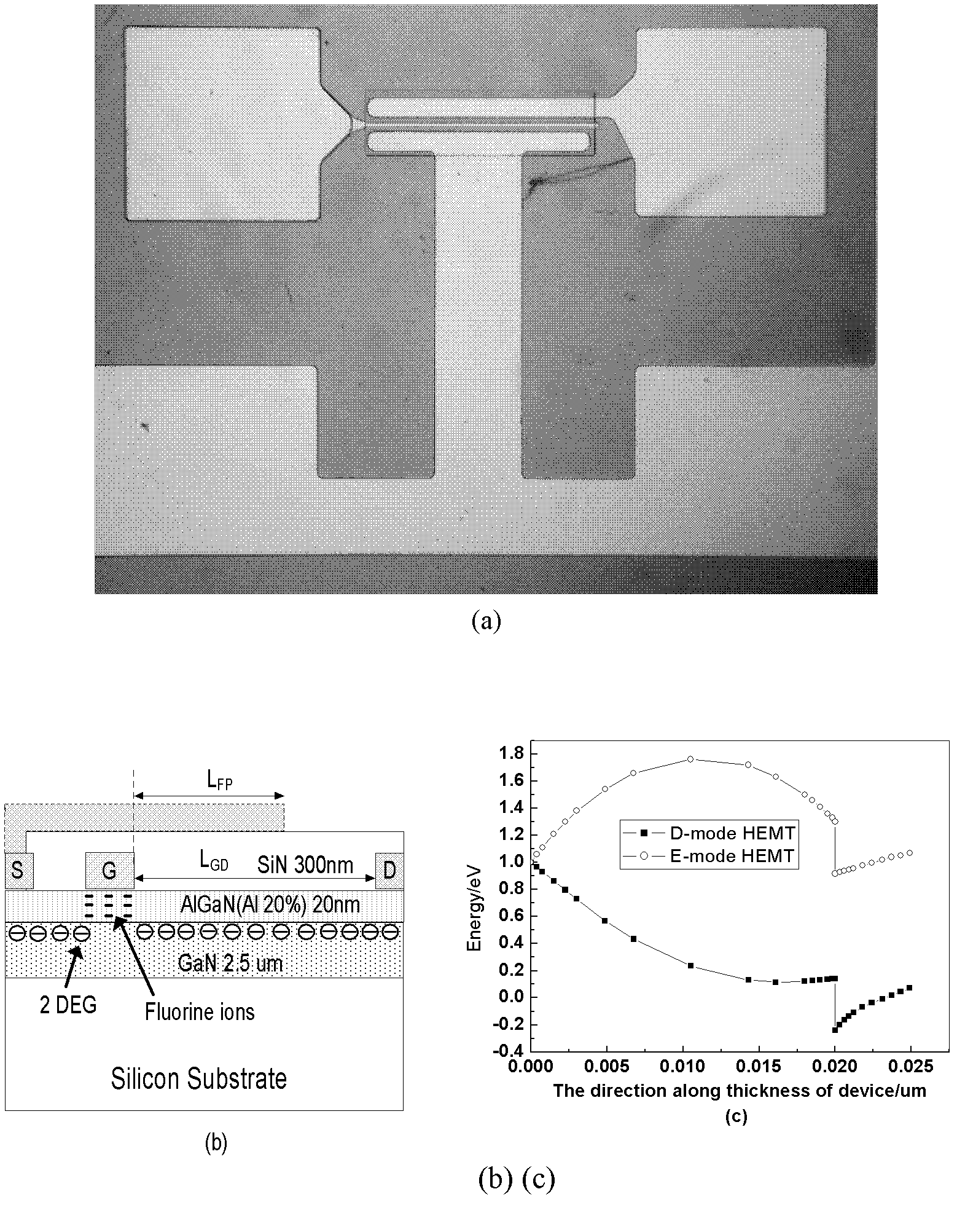
[0040] figure 2 The low-resistance silicon substrate GaN-based process platform for power electronics applications is described. The main devices include enhancement mode / depletion mode HEMTs low-voltage transistors, enhancement mode HEMTs high-voltage devices, and AlGaN / GaN SBD high-voltage Schottky diodes. Enhanced / depleted HEMTs low-voltage devices are mainly used as logic control and self-protection detection functions for chips in HVICs chips. Enhanced HEMTs devices and AlGaN SBD high-voltage Schottky diodes mainly achieve the purpose of power conversion. The high and low voltage areas adopt MESA table isolation technology. The gallium nitride process mainly includes inductively coupled plasma etching equipment STS-RIE etching to form a mesa isolation structure; sel...


PUM


Abstract

The invention discloses a process for manufacturing a gallium nitride-base GaN power integrated circuit. According to the process, current channels in a high-voltage area and a low-voltage area are cut off by the anisotropic etching of an inductively coupled plasma (ICP) etching technology to realize electric isolation in the areas. An F-ionic layer with negative charges is formed in an AlGaN potential barrier area under a metal gate Ni / Au by utilizing a reactive ion etching (RIE) autoregistration plasma etching technology, and high-density two-dimensional electron gas in a heterogenous junction is exhausted, so that an exhausted channel is converted into an enhanced channel, and the normally-closed characteristic of an AlGaN / GaN high electron mobility transistors (HEMTs) device is formed. By means of a reduced surface field (Resurf) voltage withstanding structure and a surface source field plate of an epitaxial layer GaN / silicon substrate, the electric-field distribution of a drifting area of a high-voltage device is optimized, an offset area of the device is designed, and the influence of Miller capacitance Cgd on the frequency response of the device is shielded to acquire normally-closed gallium nitride-base AlGaN / GaN (HEMTs) high-voltage device which is applied to a high-speed switch.

Description

technical field [0001] The invention relates to gallium nitride-based power electronics technology compatible with silicon technology, in particular to the development of enhanced AlGaN / GaN HEMTs high-voltage devices based on silicon substrates and monolithic gallium nitride-based integrated circuits. Background technique [0002] With the development of microelectronics technology, the performance of traditional Si and GaAs semiconductor devices has approached the theoretical limit determined by their materials themselves. The wide bandgap semiconductor gallium nitride (GaN) has a large bandgap (3.4eV), a high critical breakdown electric field (3MV / cm), and a high saturation electron drift velocity (3×10 7 cm / s), high-concentration two-dimensional electron gas (2×10 13 cm 2 ), high thermal conductivity, strong radiation resistance and good chemical stability, etc., have been used as the core components of microwave power amplification in microwave communication systems, r...

Claims


Application Information

Patent Timeline
04 Jul 2012
Publication
CN102543871A
IPC
H01L21/822; H01L21/02
Inventors
李海鸥; 黄伟