Semi-insulating silicon carbide mono-crystal

A silicon carbide single crystal, semi-insulating technology, applied in the direction of single crystal growth, single crystal growth, crystal growth, etc., can solve the problems of reducing the crystal electron mobility, affecting the crystal quality, affecting the performance of microwave devices, etc., to avoid the process of Complexity and resistivity instability, resistivity stability, effects of high crystalline quality

Active Publication Date: 2015-05-27
BEIJING TIANKE HEDA SEMICON CO LTD
View PDF10 Cites 1 Cited by
  • Summary
  • Abstract
  • Description
  • Claims
  • Application Information

AI Technical Summary

Problems solved by technology

However, transition group elements are introduced into silicon carbide crystals as deep energy levels to obtain semi-insulation, which also has some disadvantages
For example, when vanadium is introduced into SiC crystal as a deep-level dopant, the presence of a large amount of vanadium will also introduce corresponding crystal defects. When the concentration of vanadium exceeds its solid solubility limit in SiC crystal (5×10 17 cm -3 ), it will produce vanadium precipitates and micropipes, which will affect the crystallization quality of the crystal
On the other hand, if the doping amount of vanadium is too much, the electron mobility of the crystal will be reduced, which will also affect the performance of the prepared microwave device.

Method used


Image

  • Semi-insulating silicon carbide mono-crystal
  • Semi-insulating silicon carbide mono-crystal
  • Semi-insulating silicon carbide mono-crystal

Examples


Embodiment 1

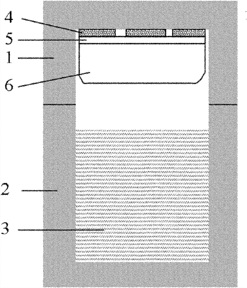
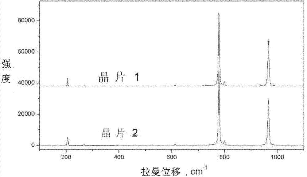
[0026] Crystal 1 is intentionally doped with a deep-level dopant (taking vanadium as an example), and its specific preparation method is as follows: add 200 mg of vanadium carbide powder (purity 99.999%) to 800 g of silicon carbide powder (purity 99.999%), Mix well and evenly with a ball mill and put it into the graphite crucible 2 as the raw material 3, cover the crucible cover 1 with the 4H-SiC seed crystal 5 bonded, and put it into the crystal growth furnace. The growth furnace is filled with argon gas, and the pressure is controlled at about 1500Pa. The temperature of the seed crystal is kept between 2000-2150°C, the temperature of the raw material is kept between 2250-2400°C, and the temperature gradient between the raw material and the seed crystal is kept between 150-300°C. The crystal growth rate is about 0.8 mm / h, and the growth ends after 15 hours and cooled to room temperature. As known to those of ordinary skill in the art, the introduction of point defects is obt...

Embodiment 2

[0036] This example adopts the same silicon carbide crystal preparation method as in Example 1. In this embodiment, the graphite crucible and heat preservation material are also purified, specifically, the graphite crucible and heat preservation material are heated to 2000° C. in an Ar atmosphere to allow impurities (such as aluminum and boron) to be fully volatilized. In this way, the influence of background impurities on crystal resistivity is minimized.

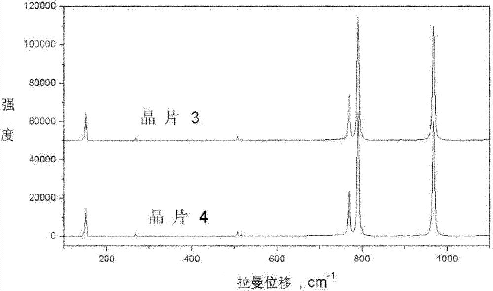
[0037] In this embodiment, crystal 3 selects vanadium as the deep level dopant. The specific preparation process is as follows: 250 mg of vanadium carbide powder (purity 99.999%) is added to 800 g of silicon carbide powder (purity 99.999%), fully mixed with a ball mill and then loaded into the graphite crucible 2 as raw material 3, and the lid is bonded A crucible lid 1 with a 6H-SiC seed crystal was removed and put into a crystal growth furnace. The growth furnace is filled with argon gas, and the pressure is controlled...


PUM

PropertyMeasurementUnit
electrical resistivityaaaaaaaaaa

Abstract

A semi-insulating silicon carbide monocrystal and a method of growing the same are disclosed. The semi-insulating silicon carbide monocrystal comprises intrinsic impurities, deep energy level dopants and intrinsic point defects. The intrinsic impurities are introduced unintentionally during manufacture of the silicon carbide monocrystal, and the deep energy level dopants and the intrinsic point defects are doped or introduced intentionally to compensate for the intrinsic impurities. The intrinsic impurities include shallow energy level donor impurities and shallow energy level acceptor impurities. A sum of a concentration of the deep energy level dopants and a concentration of the intrinsic point defects is greater than a difference between a concentration of the shallow energy level donor impurities and a concentration of the shallow energy level acceptor impurities, and the concentration of the intrinsic point defects is less than the concentration of the deep energy level dopants. The semi-insulating SiC monocrystal has resistivity greater than 1×10 5 ©·cm at room temperature, and its electrical performances and crystal quality satisfy requirements for manufacture of microwave devices. The deep energy level dopants and the intrinsic point defects jointly serve to compensate the intrinsic impurities, so as to obtain a high quality semi-insulating single crystal.

Description

technical field [0001] The invention relates to a semi-insulating silicon carbide single crystal, in particular to a semi-insulating silicon carbide substrate used in microwave devices. Background technique [0002] Silicon carbide (SiC) materials have huge applications in high temperature, high frequency, high power, optoelectronics and radiation resistance due to their wide band gap, high critical breakdown electric field, high thermal conductivity, and high carrier saturation drift velocity. prospect. In particular, semi-insulating silicon carbide substrates are widely used in the field of microwave devices. The "semi-insulating" refers to the resistivity at room temperature greater than 10 5 Ω·cm, which is consistent with the conceptual description of "high resistance". Transistors fabricated from semi-insulating silicon carbide are capable of generating more than five times the power density of GaAs microwave components at frequencies up to 10 GHz. Therefore, the man...

Claims


Application Information

Patent Timeline
Patent Type & Authority Patents(China)
IPC IPC(8): C30B29/36H01L29/24H01L29/38H01L29/772
CPCC30B23/00C30B29/36C30B23/005H01L29/435C30B23/002C30B23/06H01L21/02529H01L29/1608
Inventor 陈小龙刘春俊彭同华李龙远王刚刘宇
Owner BEIJING TIANKE HEDA SEMICON CO LTD
Why Eureka
Try Eureka