

Method of surface self-assembly of graphene/polyimide transparent electric conduction film
A transparent conductive film, polyimide technology, applied in cable/conductor manufacturing, conductive layers on insulating carriers, circuits, etc., can solve the incompatibility between inorganic conductive layers and organic substrates, flexible substrates and deposition layers. Weak adhesion and other problems, to achieve the effect of improving incompatibility, firm interface bonding, and good transmittance
- Summary
- Abstract
- Description
- Claims
- Application Information
AI Technical Summary
Problems solved by technology
Method used
Image


Examples
specific Embodiment approach 1
[0014] Specific embodiment one: the method for surface self-assembled graphene / polyimide transparent conductive film in the present embodiment is carried out according to the following steps:
[0015] Step 1. Put 0.05~0.1g of graphite oxide with a mass purity of more than 99.9% into 100mL of N,N-dimethylacetamide (DMAc) or N-methylpyrrolidone (NMP), ultrasonically disperse for 60min, and then add A reducing agent, the reduction reaction is carried out at 120-130° C. for 1-2 hours to obtain a graphene organic solution system (the graphene organic solution system is stored at room temperature for more than 30 days);
[0016] Step 2, gradually add 0.02mol aromatic dianhydride monomer and 0.02mol aromatic diamine monomer into 100mL N,N-dimethylacetamide (DMAC) solvent, mechanically stir for 5 hours in an inert atmosphere (intrinsic viscosity reaches 40dL / g), thereby obtaining PAA solution;
[0017] Step 3, the graphene organic solution system obtained in step 1 and the PAA soluti...
specific Embodiment approach 2
[0018] Embodiment 2: The difference between this embodiment and Embodiment 1 is that the graphite oxide described in Step 1 is obtained by oxidizing natural flake graphite by chemical oxidation. Other steps and parameters are the same as in Embodiment 1
specific Embodiment approach 3
[0019] Embodiment 3: The difference between this embodiment and Embodiment 1 or 2 is that the reducing agent in step 1 is hydrazine or sodium borohydride, the amount of hydrazine is 1 mL, and the amount of sodium borohydride is 0.1 g. Other steps and parameters are the same as those in Embodiment 1 or Embodiment 2.
PUM
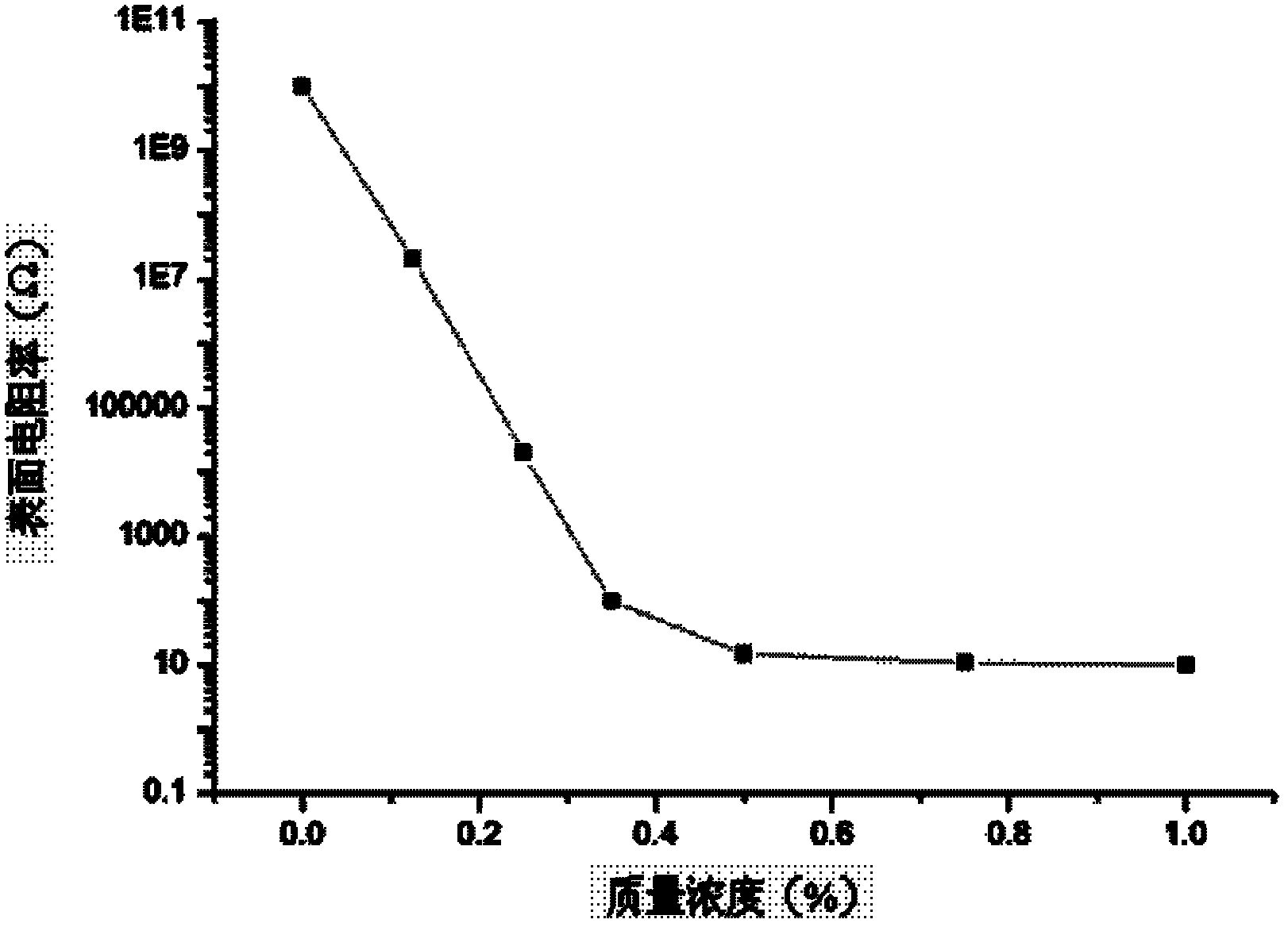
| Property | Measurement | Unit |
|---|---|---|
| Surface resistance | aaaaa | aaaaa |
| Surface resistance | aaaaa | aaaaa |
| Surface resistance | aaaaa | aaaaa |
Abstract
Description
Claims
Application Information