Preparation method of carbon microelectrode array structure

An array structure and carbon microelectrode technology, which is applied in the direction of microstructure technology, microstructure devices, and manufacturing microstructure devices, can solve the problems of generating wrinkles and not considering the preparation of nano-fold structures, and achieve fine graphics, long service life, The effect of increasing the surface area

Inactive Publication Date: 2015-03-04
HUAZHONG UNIV OF SCI & TECH
View PDF5 Cites 2 Cited by
  • Summary
  • Abstract
  • Description
  • Claims
  • Application Information

AI Technical Summary

Problems solved by technology

[0007] In terms of the preparation process of film wrinkles, Xie et al. proposed in the article "Encoding localized strain history through wrinkle based structural colors" (Advanced Material, 2010, 22:4390-4394) to use shape memory polymer to make the substrate and heat it to transform After the temperature is high, the microstructure is made on the surface of the substrate by imprinting technology, then the temperature is lowered and the metal film is deposited, and finally the temperature is raised to the transition temperature. At this time, the metal film on the side wall of the microstructure will buckle and form wrinkles, but this method cannot Generate wrinkles across the surface
Many other different manufacturing processes have also been proposed, but the research on these thin film wrinkle generation processes is carried out on a flat surface, without considering the preparation of nano-wrinkle structures on the basis of existing micro-technical processing to realize the manufacture of micro-nano integrated structures.

Method used


Image

  • Preparation method of carbon microelectrode array structure
  • Preparation method of carbon microelectrode array structure
  • Preparation method of carbon microelectrode array structure

Examples


Embodiment 1

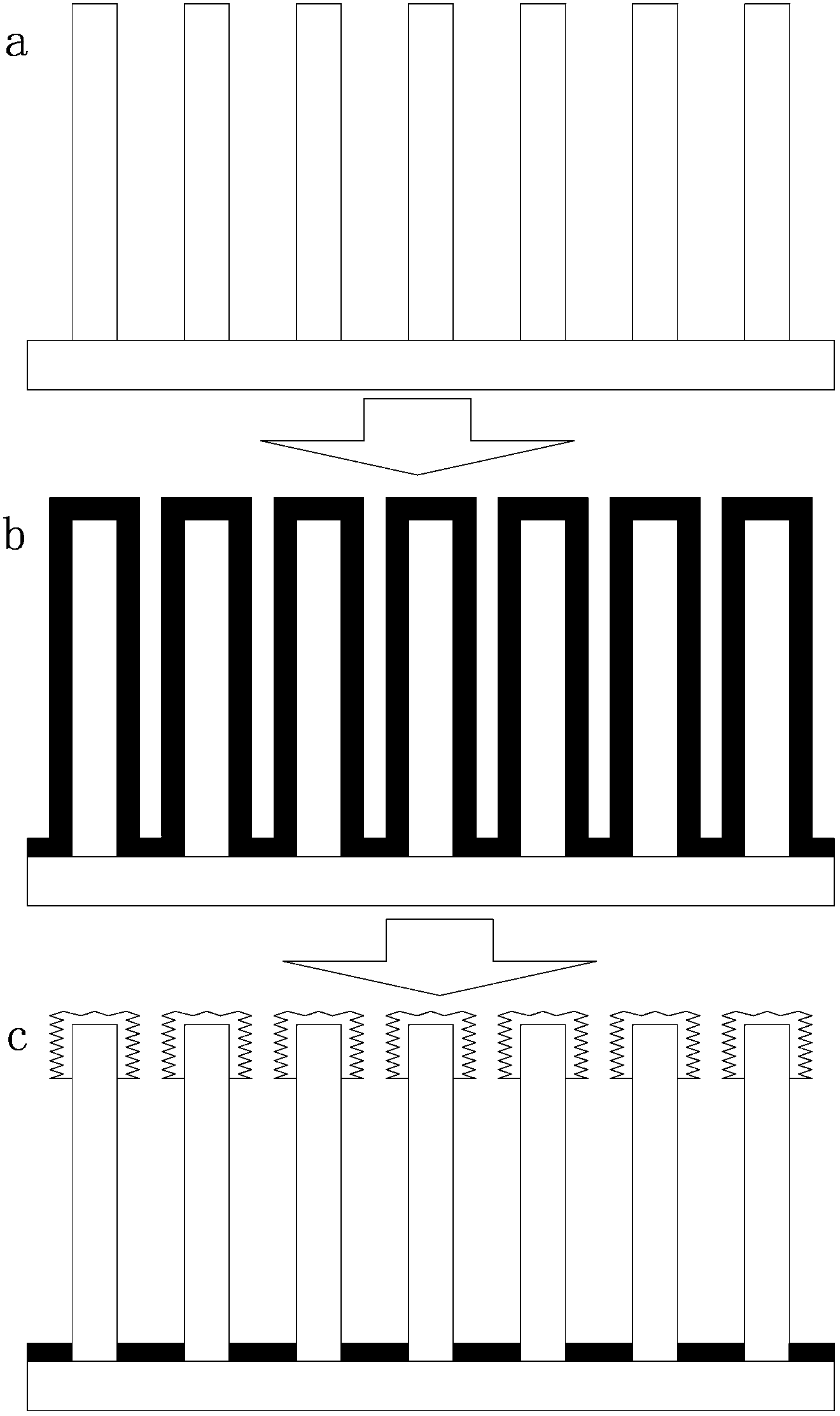
[0036] (1) Photolithography steps:

[0037] (1.1) Cleaning steps: Clean a 2-inch silicon wafer ultrasonically for 10 minutes with acetone, put it in SPM (mixed solution of concentrated sulfuric acid and hydrogen peroxide), heat and clean it at 80°C for 15 minutes, and then clean it thoroughly with deionized water Finally, place it on a 200°C hot plate and bake it for 15 minutes to make it completely dry;

[0038] (1.2) Homogenization step: Coat SU-82100 negative photoresist on the cleaned silicon substrate on the KW-4A type homogenizer (diluted with relevant diluents such as propylene glycol methyl ether acetate (PGMEA)), The homogenization is carried out in two steps. The homogenization machine first rotates at a low speed of 500r / min for 50s, and then rotates at a high speed of 1000r / min for 100s. The function is to volatilize the solvent and fix the adhesive layer to prepare for better exposure. If the pre-baking is insufficient, it will easily lead to the adhesion of the ad...

Embodiment 2

[0057] The relevant steps are the same as those in Example 1, except that in step (7), instead of depositing nickel, a layer of aluminum is deposited with a thickness of about 500 nm during metal deposition. In this embodiment, the main process parameters of one-step pyrolysis are listed in Table 3.

[0058] The one-step pyrolysis process parameter of table 3 embodiment 2

[0059]

[0060]

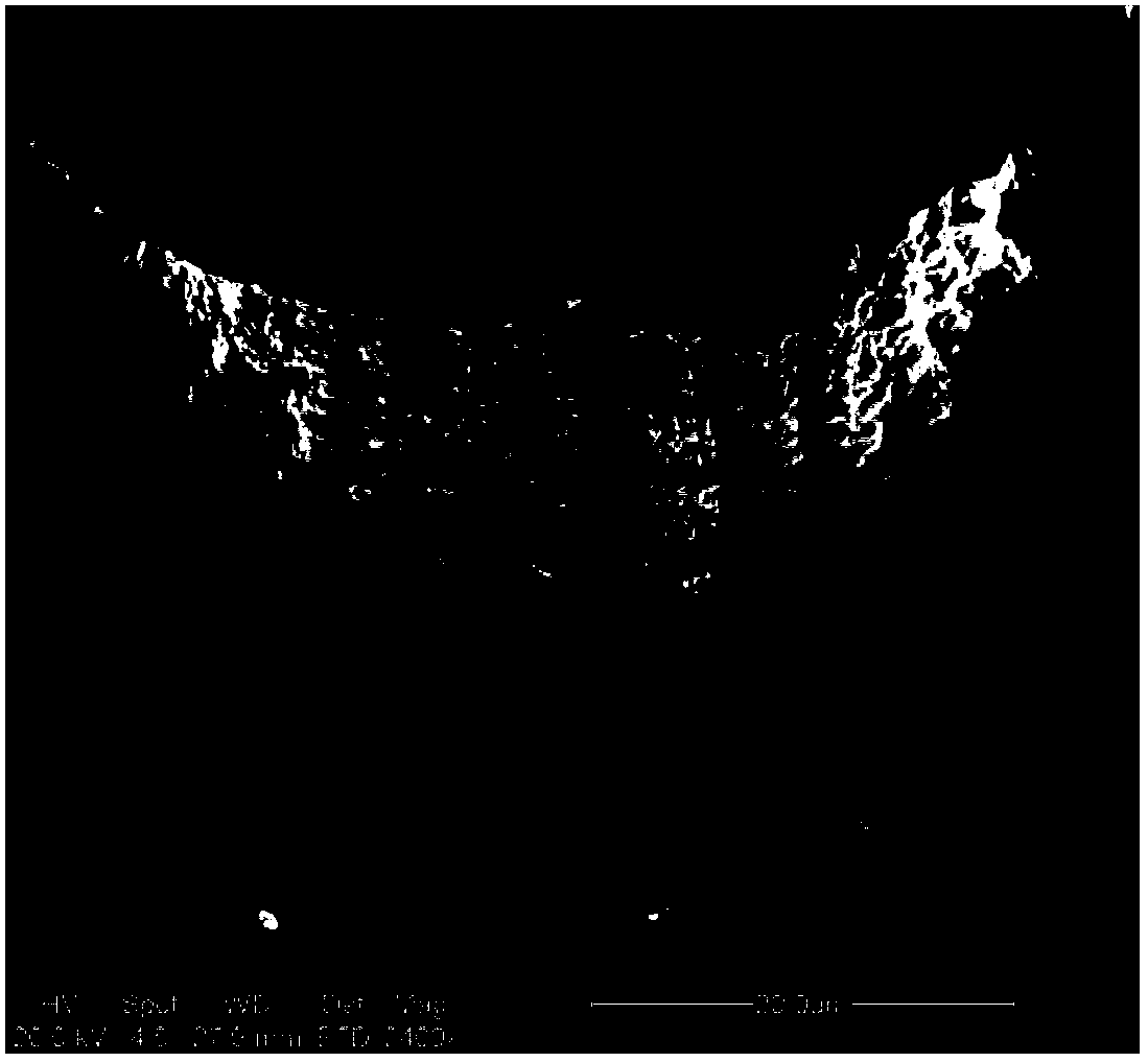
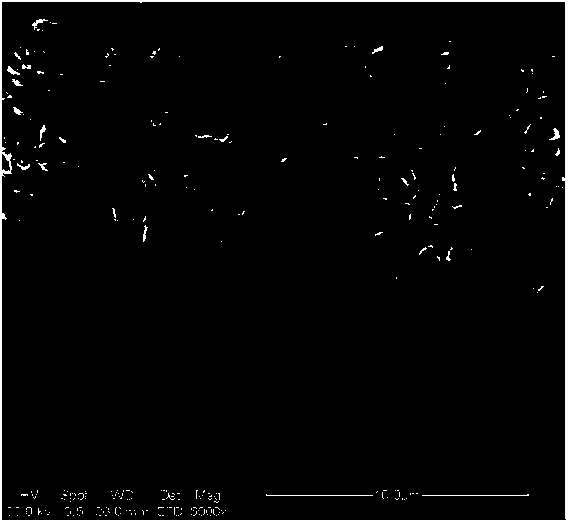
[0061] After pyrolysis, a carbon microstructure array with a large amount of integrated metal nanofold structure on the surface is also obtained, as shown in Figure 3(a) and Figure 3(b), and the metal nanofold growth site after pyrolysis is shown in Figure 3(a) As shown, the growth of metal nanofolds on carbon pillars is shown in Fig. 3(b).

Embodiment 3

[0063] The relevant steps are the same as in Example 1, except that in step (7), when metal is deposited, instead of depositing a single layer of metal, a double layer is deposited, first depositing a layer of nickel with a thickness of about 500nm, and then depositing a layer of nickel on the nickel , and then deposit a layer of aluminum, the thickness of which is also about 500nm.

[0064] A carbon microstructure array with a large number of integrated metal nanofold structures on the surface was prepared through the above process, as shown in Figure 3(a) and Figure 3(b). The array after pyrolysis is shown in Figure 3(a), and 3(b) shows more clearly the results of growing nanostructures from single carbon pillars. It can be seen from Figure 3(a) that there is no adhesion between carbon pillars. Combining Figure 3(a) and Figure 3(b), a large number of metal nanofold structures are grown on the surface of the carbon pillar and a small area around it.

[0065] Compared with t...


PUM

PropertyMeasurementUnit
melting pointaaaaaaaaaa
thicknessaaaaaaaaaa

Abstract

The invention belongs to the technical field of carbon micro electro mechanical system, and provides a preparation method of a carbon microelectrode array structure. The method comprises steps of: (1) photolithography to obtain a carbon micro structure part of the array; (2) metal precipitation: precipitating one or more metal layers on the surface of the obtained carbon micro structure; and (3) pyrolysis: carrying out multiple steps of pyrolysis in an inert gas atmosphere or inert mixed gas atmosphere and at different temperatures. According to the above steps, carbon microelectrode array structure with nano structure integrated on the surface can be grew and obtained. The method of the invention combines thick photoresist lithography, metal precipitation and pyrolysis, so that the obtained micro-nano integrated structure has large specific surface area. The method of the present invention can be used in a micro electro mechanical system, and has the advantages of simple technology, low cost, high controllability, mass growth and good structure. The obtained micro-nano integrated structure has good electrical properties, and can be used as a motor and be widely applied to microcomputer fields, such as the minicell and micro electrochemical sensor, etc.

Description

technical field [0001] The invention belongs to the field of carbon micro-electromechanical technology, and in particular relates to a method for preparing a carbon micro-electrode array structure with micro-nano metal folds integrated on the surface. The prepared array structure can be used as a micro-electrode and applied to micro-batteries, biochips and micro-electrochemistry Sensors and other micro-electromechanical fields. Background technique [0002] Carbon Micro-Electro-Mechanical Systems (C-MEMS) technology is a manufacturing technology of thick-resist lithography combined with high-temperature pyrolysis (usually around 1000 degrees), which is based on high-viscosity photoresist (such as SU-8 glue) and conventional photoresist The three-dimensional cross-linked microstructure is generated by the engraving process, and then the cross-linked structure is pyrolyzed into a glassy carbon structure by controlling the temperature rise in a pyrolysis furnace and an inert at...

Claims


Application Information

Patent Timeline
Patent Type & Authority Patents(China)
IPC IPC(8): B81C1/00
Inventor 汤自荣史铁林徐亮亮龙胡习爽刘丹夏奇廖广兰
Owner HUAZHONG UNIV OF SCI & TECH
Why Eureka
Try Eureka