

Vertical-channel mixed-lattice-strain BiCMOS (bipolar complementary metal oxide semiconductor) integrated device and preparation method
An integrated device, vertical channel technology, applied in semiconductor/solid-state device manufacturing, electric solid-state devices, semiconductor devices, etc., can solve the problem that the mobility cannot be optimized at the same time
- Summary
- Abstract
- Description
- Claims
- Application Information
AI Technical Summary
Problems solved by technology
Method used
Image

Examples
Embodiment 1
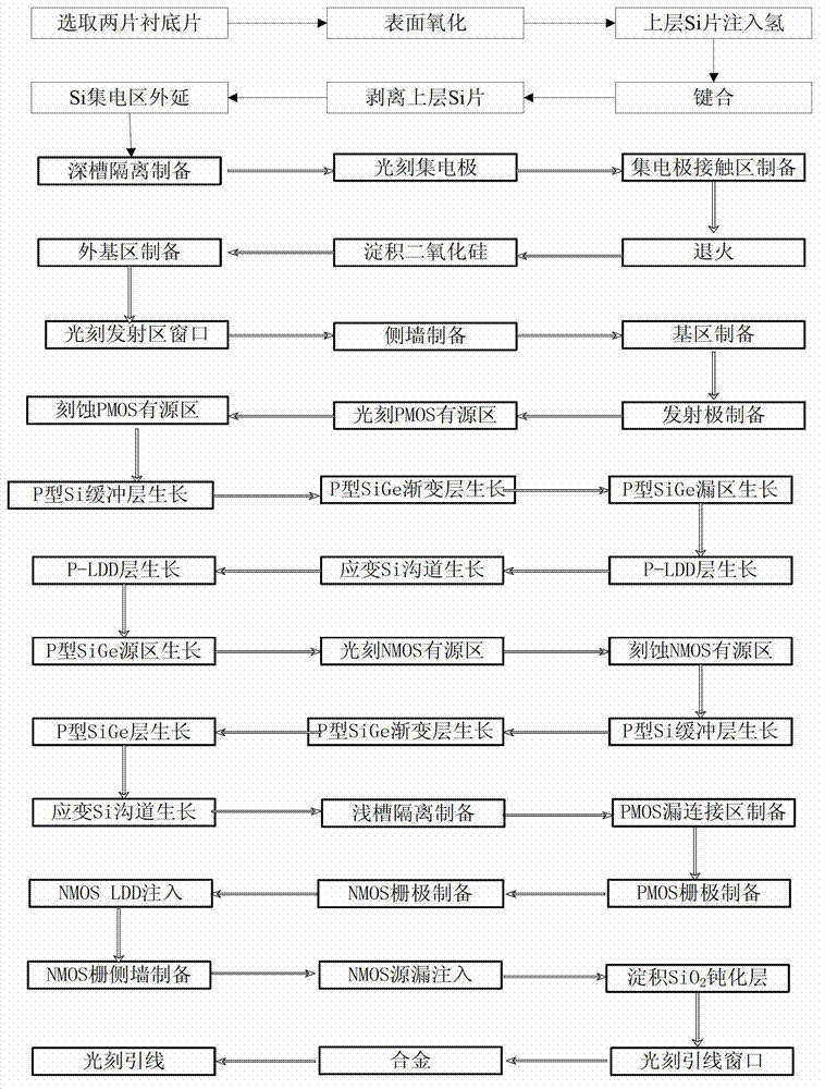
[0137] Embodiment 1: Preparation of a vertical channel with a channel length of 22nm, a mixed crystal plane strained BiCMOS integrated device and a circuit, the specific steps are as follows:
[0138] Step 1, SOI substrate material preparation.
[0139] (1a) Select the P-type doping concentration as 1×10 15 cm -3 The Si sheet with a crystal plane of (100) is oxidized on the surface, and the thickness of the oxide layer is 0.5 μm, which is used as the base material of the upper layer, and hydrogen is injected into the base material;
[0140] (1b) Select the N-type doping concentration as 1×10 15 cm -3 The Si sheet with a crystal plane of (110) is oxidized on the surface, and the thickness of the oxide layer is 0.5 μm, which is used as the base material of the lower layer;
[0141] (1c) Using a chemical mechanical polishing (CMP) process to polish the surface of the lower layer and the upper layer of substrate material after hydrogen injection;
[0142] (1d) SiO on the surf...
Embodiment 2
[0214] Embodiment 2: The preparation of a vertical channel with a channel length of 30nm, a mixed crystal plane strain BiCMOS integrated device and a circuit, the specific steps are as follows:
[0215] Step 1, SOI substrate material preparation.
[0216] (1a) Select the P-type doping concentration as 3×10 15 cm -3 The Si sheet with a crystal plane of (100) is oxidized on the surface, and the thickness of the oxide layer is 0.75 μm, which is used as the base material of the upper layer, and hydrogen is injected into the base material;
[0217] (1b) Select the N-type doping concentration as 3×10 15 cm -3 The Si sheet with a crystal plane of (110) is oxidized on the surface, and the thickness of the oxide layer is 0.75 μm, which is used as the base material of the lower layer;
[0218] (1c) Using a chemical mechanical polishing (CMP) process to polish the surface of the substrate material of the lower layer and the upper layer of the active layer after injecting hydrogen, re...
Embodiment 3
[0291] Embodiment 3: The preparation of a vertical channel with a channel length of 45nm, a mixed crystal plane strained BiCMOS integrated device and a circuit, the specific steps are as follows:
[0292] Step 1, SOI substrate material preparation.
[0293] (1a) Select the P-type doping concentration as 5×10 15 cm -3 Si wafers with a crystal plane of (100) are oxidized on the surface, and the thickness of the oxide layer is 1 μm, which is used as the base material of the upper layer, and hydrogen is injected into the base material;
[0294] (1b) Select the N-type doping concentration as 5×10 15 cm -3 The Si sheet with a crystal plane of (110) is oxidized on its surface, and the thickness of the oxide layer is 1 μm, which is used as the base material of the lower layer;
[0295] (1c) Using a chemical mechanical polishing (CMP) process to polish the lower layer and the surface of the upper substrate material after hydrogen injection;
[0296] (1d) SiO on the surface of the ...
PUM
 Abstract
Description
Claims
Application Information