Preparation method for bismuth titanate nanowire solar cells

A solar cell, bismuth ferrite nanotechnology, applied in the manufacture of circuits, electrical components, final products, etc.

Active Publication Date: 2013-01-02
南通东湖国际商务服务有限公司
View PDF6 Cites 16 Cited by
  • Summary
  • Abstract
  • Description
  • Claims
  • Application Information

AI Technical Summary

Problems solved by technology

[0003]In 2009, Choi et al. found that there is a large photovoltaic effect in the multiferroic material BiFeO3 single crystal, which has a narrow Optical bandgap (2.2 eV), high saturation polarization (90 μC / cm2), which makes the application of BiFeO3 materials in photovoltaic devices possible, However, the photocurrent density generated by it is small (7.35 μA / cm2), which directly leads to the low photoelectric conversion efficiency of BiFeO3 materials[T. Choi, S. Lee, Y. J. Choi, V. Kiryukhin, and S. W. Cheong, Science,324, 63 (2009).]; In addition, the research on the photovoltaic effect of BiFeO3 thin films shows that BiFeO3 The film has a wide optical band gap (around 2.7 eV) and a high open circuit voltage (0.3-0.9 V) [W. Ji, K. Yao, and Y. C. Liang, Adv. Mater. 22, 1763 (2010) . S. Y. Yang, L. W. Martin, S. J. Byrnes, T. E. Conry, S. R. Basu, D. Paran, L. Reichertz, J. Ihlefeld, C. Adamo, A. Melville, Y. H. Chu, C. H. Yang, J. L. Musfeldt, D. G. Schlom, J. W. Ager III, and R. Ramesh, Appl. Phys. Lett. 95, 062909 (2009).]; however, the BiFeO 3Optical Bandgap of Thin Films[K. Jiang, J. J. Zhu,J. D. Wu, J. Sun, Z. G. Hu, and J. H. Chu, ACS Applied Materials & Interfaces, 3, 4844 (2011). Z. Fu, Z. G. Yin, N. F. Chen, X. W. Zhang, H. Zhang, Y. M. Bai, and J. L. Wu, Phys. Status Solidi RRL , 6, 37 (2012).]; another study showed that the polycrystalline BiFeO3 film has a narrow optical bandgap (2.2 eV) and a large photocurrent density (2.8 mA / cm 2) [Y. Y. Zang, D. Xie, X. Wu, Y. Chen, Y. X. Lin, M. H. Li, H. Tian, ​​X. Li, Z. Li, H. W. Zhu, T. L. Ren, and D. Plant, Appl. Phys. Lett. 99, 132904 (2011).]; Electrode materials have a great influence on the optical properties of polycrystalline BiFeO3 thin films, polycrystalline BiFeO using oxide electrode materials 3Thin films have greater photovoltaic effect than metal materials [B. Chen, M. Li, Y. W. Liu, Z. H. Zuo, F. Zhuge, Q. F. Zhan, and R. W. Li, Nanotechnology, 22, 195201 (2011).]; In addition, studies on the optical properties of BiFeO3 nanowires also show that it has a lower optical bandgap (2.5 eV) [F. Gao, Y. Yuan, K. F. Wang, X. Y. Chen, F. Chen, J. M. Liu, and Z. F. Ren, Appl. Phys. Lett. 89, 102506 (2006).]; it can be seen that there have been many reports on the photovoltaic effect of BiFeO3 materials , but most of the BiFeO3 materials involved are bulk materials or thin film materials, and there are few reports on the optical properties of BiFeO3 with low-dimensional structures, although there are currently several The literature reports the preparation and optical properties of BiFeO3 nanowires, but only pure BiFeO3 nanowire arrays are involved. The open circuit voltage, photocurrent density The study of electrical properties has not been reported, let alone the report of BiFeO3 nanowire solar cells with other structures

Method used


Image

  • Preparation method for bismuth titanate nanowire solar cells

Examples


specific Embodiment 1

[0029] 1. High-purity Al sheet annealing

[0030] Annealing temperature is 500 0 C, the annealing time is 4 hours, take it out after cooling to room temperature with the furnace.

[0031] 2. ultrasonic cleaning

[0032] Sonicate with acetone, ethanol, and deionized water for 3 minutes in sequence to remove stains on the surface of the Al sheet.

[0033] 3. remove natural oxide layer

[0034] With 2 mol / L NaOH solution, the temperature is 60 0 C, the soaking time is 2 minutes, then take out and rinse with deionized water to remove the natural oxide layer.

[0035] 4. electrochemical polishing

[0036] Put the Al sheet into a mixed solution of 5vol% sulfuric acid, 95vol% phosphoric acid and 20 g / L chromic acid, use a stirring device to circulate the mixed solution, perform electrochemical polishing for 5 minutes, and the temperature of the water bath is 85 0 C, the polishing current is 0.8 A, and then it is taken out and cleaned with deionized water.

[00...

specific Embodiment 2

[0056] The difference between this embodiment and the specific example 1 is that in step 5, the voltage of anodic oxidation is changed to 10 V, 25 V, 60 V, and 100 V respectively, and then the pore sizes are respectively 20 nm, 35 nm, 80 nm, and 120 nm. nm porous alumina template, other steps and parameters are the same as those in Embodiment 1.

[0057] Implementation effect: get BiFeO 3 The optical bandgap of the nanowire is 2.4 eV, at AM 1.5, 100 mW / cm 2 Under the irradiation of standard light intensity, the short-circuit current density is 6-8 mA / cm 2 , the open circuit voltage is 0.8-1 V, and the efficiency is 0.8-1.2%.

specific Embodiment 3

[0059] The difference between this embodiment and the specific example 1 is that in step 7, the double-pass porous alumina template is immersed in 6wt% phosphoric acid to expand the pores for 5-40 minutes, and a double-pass alumina template with a pore size of 60-200 nm can be obtained. Other steps and parameters are the same as those in the first embodiment.

[0060] Implementation effect: get BiFeO 3 The optical bandgap of the nanowire is 2.4 eV, at AM 1.5, 100 mW / cm 2 Under the irradiation of standard light intensity, the short-circuit current density is 6-7 mA / cm 2 , the open circuit voltage is 0.8-0.9 V, and the efficiency is 0.8-1%.


PUM

PropertyMeasurementUnit
thicknessaaaaaaaaaa
thicknessaaaaaaaaaa

Abstract

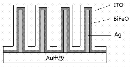
The invention belongs to the technical field of semiconductor materials, and in particular relates to a preparation method for bismuth titanate nanowire solar cells. By utilizing a BiFeO3 nanowire structure, the optical band gap is decreased and the absorption on sunshine is improved; the collection capacity of carriers is improved by utilizing Ag nanowires and electrodes on an ITO, so that the purpose of improving the photoelectricity conversion efficiency of the bismuth titanate nanowire solar cells can be achieved.

Description

technical field [0001] The invention belongs to the technical field of semiconductor materials, in particular to a BiFeO 3 Preparation method of nanowire solar cell. Background technique [0002] At present, traditional silicon-based solar cells use p-n junctions or Schottky junctions to separate electron-hole pairs, and the light-induced voltage is limited by the high energy barrier in the interface region, resulting in a small open-circuit voltage; secondly, in order to To improve the conversion efficiency of the cell, it is usually necessary to design a special anti-reflection structure and passivate the surface to increase the absorption of sunlight; more importantly, the price of silicon raw materials determines the manufacturing cost of silicon-based solar cells Expensive; therefore, silicon-based solar cells have disadvantages such as low open circuit voltage, complex structural design, and expensive manufacturing costs; however, another mechanism of photovoltaic eff...

Claims


Application Information

Patent Timeline
Patent Type & Authority Applications(China)
IPC IPC(8): H01L31/18H01L31/20
CPCY02P70/50
Inventor 邱建华丁建宁袁宁一陈智慧王秀琴
Owner 南通东湖国际商务服务有限公司
Why Eureka
Try Eureka