Method for preparing cone-shaped structure on gallium phosphide (GaP) surface

A cone-shaped and equipment technology, which is applied in the preparation and application of three-dimensional micro-nano structures, can solve problems such as the inability to realize high-aspect-ratio cone-shaped structures, and the inability to effectively control cone-shaped structures, and achieve high-depth effects

Active Publication Date: 2013-07-10
INST OF PHYSICS - CHINESE ACAD OF SCI
View PDF5 Cites 18 Cited by
  • Summary
  • Abstract
  • Description
  • Claims
  • Application Information

AI Technical Summary

Problems solved by technology

[0004] The technical problem to be solved: to solve the defects that the shape, size and period of the conical structure cannot be effectively controlled by the previous wet processing method, and ...

Method used


Image

  • Method for preparing cone-shaped structure on gallium phosphide (GaP) surface
  • Method for preparing cone-shaped structure on gallium phosphide (GaP) surface
  • Method for preparing cone-shaped structure on gallium phosphide (GaP) surface

Examples


Embodiment 1

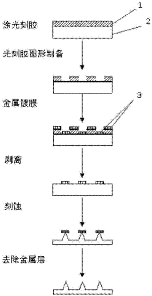
[0029] Embodiment 1: as figure 1 A flowchart showing the preparation of a tapered structure on the surface of GaP using photoresist pattern preparation technology, metal coating, stripping and etching processes in the embodiment of the present invention includes the following steps:

[0030] Step S1: Spin-coat photoresist on the surface of the GaP sample, and use one of UV exposure, electron beam exposure, laser interference exposure, laser direct writing, and nanoimprinting techniques to prepare a photoresist with a porous structure on the photoresist Array pattern, obtain the sample with photoresist pattern;

[0031] Step S2: Put the sample with photoresist pattern into one of thermal evaporation equipment, electron beam evaporation equipment, and sputtering equipment for coating, and grow a metal among chromium, aluminum, gold, titanium, and nickel as the engraved Etch the mask to obtain a sample with a metal layer.

[0032] Step S3: putting the sample with the metal laye...

Embodiment 2

[0035] Embodiment 2: Utilizing the preparation method of the present invention, adopting electron beam exposure, metal coating, stripping and etching techniques to prepare a cone-shaped structure on the GaP surface, specifically comprising the following steps:

[0036] Step 1) Spin-coat electron beam photoresist ZEP520 on the GaP surface, and bake the sample on a hot plate at 180°C for 2 minutes after spin-coating;

[0037] Step 2) using electron beam exposure equipment to prepare a circular hole array photoresist pattern on the photoresist;

[0038] Step 3) put the sample with photoresist pattern prepared in step 2) into a thermal evaporation device to grow a 50nm thick metal chromium film;

[0039] Step 4) putting the sample after growing the metal layer into an acetone solution for stripping to obtain a chromium frustum array;

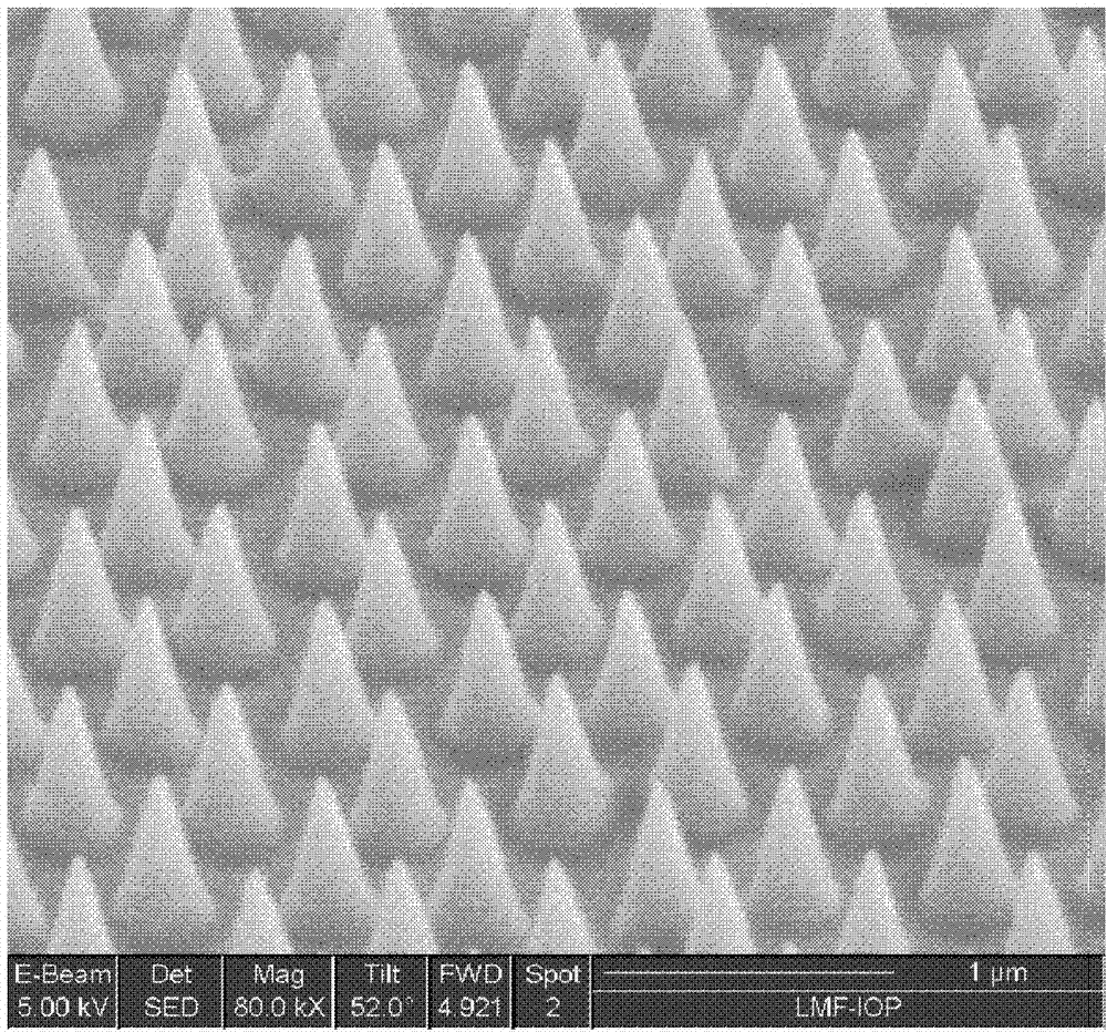
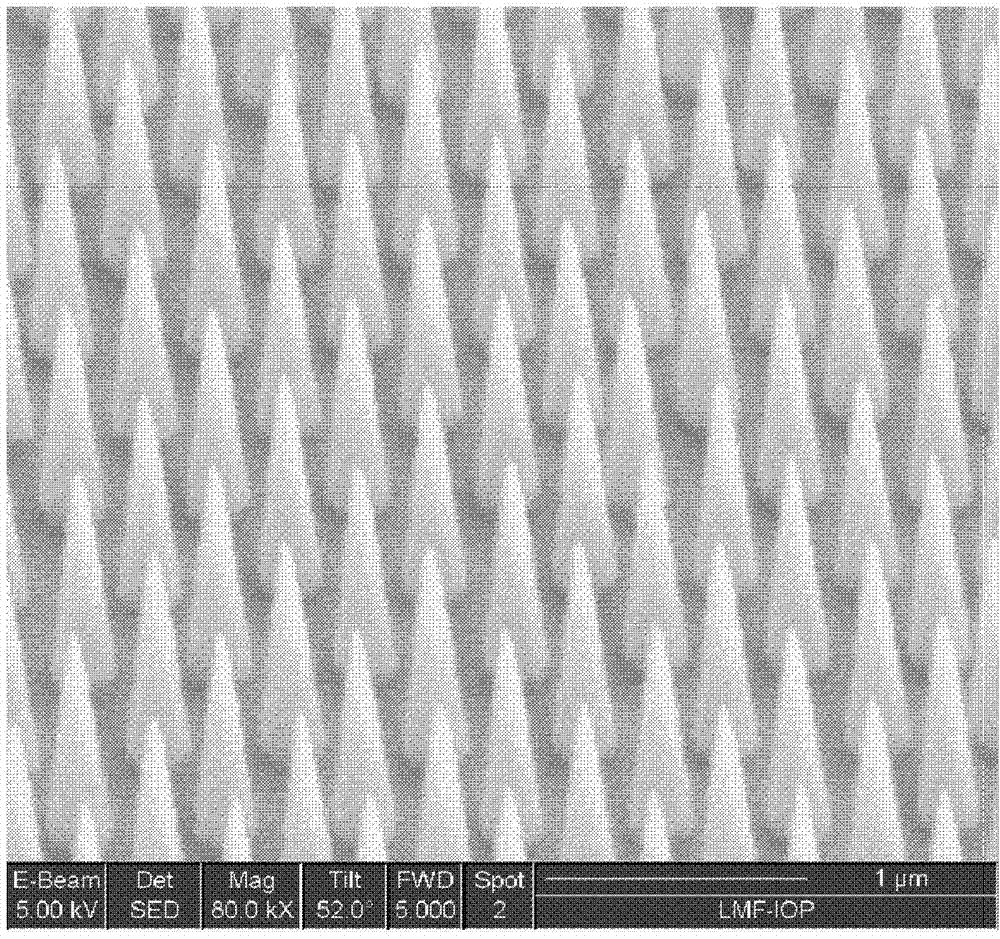
[0040] Step 5) put the sample obtained in step 4) into an inductively coupled plasma etching device, and the etching parameters used are: chlorine...

Embodiment 3

[0042] Embodiment 3: In this embodiment, nano-imprinting, metal coating, stripping and etching techniques are used to prepare a pyramidal structure with a high aspect ratio on the GaP surface with a silicon nitride sacrificial layer grown on the surface, specifically including the following steps:

[0043] Step 1: grow a silicon nitride film with a thickness of 200nm on the surface of the GaP sample by plasma enhanced chemical vapor deposition (PECVD) as a sacrificial mask for etching;

[0044] Step 2: Spin-coat polymethyl methacrylate PMMA photoresist on the surface of the sample, and bake the sample on a hot plate at 180°C for 1 minute after spin-coating;

[0045] Step 3: Prepare a photoresist pattern with a circular hole array on the photoresist using a nanoimprinting device;

[0046] Step 4: put the sample into the electron beam evaporation equipment, and evaporate a layer of gold film with a thickness of 100nm;

[0047] Step 5: put the vapor-deposited sample into an aceton...


PUM

PropertyMeasurementUnit
Thicknessaaaaaaaaaa

Abstract

The invention provides a method for preparing a cone-shaped structure on a gallium phosphide (GaP) surface. Photoresist is coated on the surface of a GaP sample in a spinning mode, and then a micrometer/nanometer scale image preparation technology is used for preparing a hole-shaped photoresist array pattern on the photoresist to obtain a sample with the hole-shaped photoresist array pattern; metal plating equipment is used for growing a metal layer on the sample with the hole-shaped photoresist array pattern, and a desolventizing process is carried out to obtain a sample with a metal-column-shaped pattern array; dry etching equipment is used for carrying out etching on the sample with the metal-column-shaped pattern array to obtain a GaP sample of a cone-shaped array structure; and the GaP sample of the cone-shaped array structure is placed in metal corrosive liquid to be cleaned, residual metal layers on the surface of the GaP sample of the cone-shaped array structure are removed, and then a cone-shaped array structure is obtained on the Gap surface. The cone-shaped array structure can be used for improvement of light extraction efficiency of an AlGaInP-based red light-emitting diode (LED).

Description

technical field [0001] The invention relates to the preparation and application fields of three-dimensional micro-nano structures, in particular to a method for preparing cone-shaped structures on the surface of gallium phosphide (GaP) based on photoresist pattern preparation, metal coating, stripping and etching processes, and is used for aluminum Enhancement of light extraction efficiency of gallium indium phosphide (AlGaInP) based red LEDs. Background technique [0002] Light-emitting diodes (LEDs) are being used more and more in many fields. At the same time, improving the luminous efficiency of LEDs is also a hot topic that everyone has been paying attention to. The luminous efficiency of LEDs is mainly divided into internal quantum efficiency and external quantum efficiency. External quantum efficiency is the product of internal quantum efficiency and light extraction efficiency. Therefore, the key to improving LED luminous efficiency Two basic approaches are to impro...

Claims


Application Information

Patent Timeline
IPC IPC(8): H01L33/00H01L33/22
Inventor 杨海方刘哲顾长志尹红星夏晓翔
Owner INST OF PHYSICS - CHINESE ACAD OF SCI
Why Eureka
Try Eureka