Method for preparing porous silicon-based one-dimensional nanowire gas sensitive element

A tungsten oxide nanowire and porous silicon-based technology, applied in the field of gas sensor, can solve the problem of high working temperature, achieve high response value, mature manufacturing process, and low price

Inactive Publication Date: 2013-08-14
TIANJIN UNIV
View PDF8 Cites 15 Cited by
  • Summary
  • Abstract
  • Description
  • Claims
  • Application Information

AI Technical Summary

Problems solved by technology

The present invention adopts the chemical vapor deposition method to combine the ordered porous silicon and the one-dimensional tungsten oxide nanostructure to form a new composite structure gas-sensing material, which has a huge specific surface area and a large surface activity, and provides a large amount of The gas adsorption position and

Method used


Image

  • Method for preparing porous silicon-based one-dimensional nanowire gas sensitive element
  • Method for preparing porous silicon-based one-dimensional nanowire gas sensitive element
  • Method for preparing porous silicon-based one-dimensional nanowire gas sensitive element

Examples


Embodiment 1

[0033] 1) Clean the silicon substrate substrate:

[0034] A 2-inch p-type single-sided polished single-crystal silicon wafer with a resistivity of 10Ω·cm, a thickness of 400μm, and a (100) crystal orientation was cut into a rectangular silicon substrate with a size of 2.4cm×0.9cm, which was sequentially passed through concentrated sulfuric acid and Soak in hydrogen peroxide mixed solution for 30 minutes, soak in hydrofluoric acid aqueous solution for 20 minutes, ultrasonically clean with acetone solvent for 15 minutes, ultrasonically clean with absolute ethanol for 15 minutes, and ultrasonically clean in deionized water for 10 minutes;

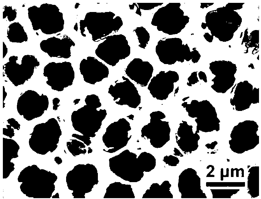
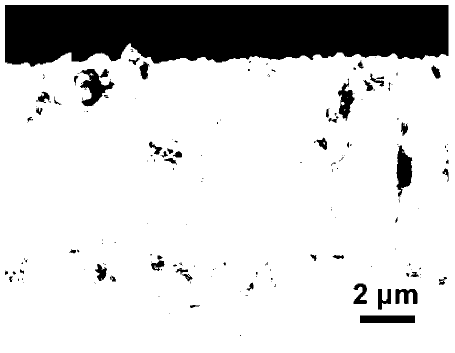
[0035] 2) Preparation of silicon-based porous silicon with micron-sized pores:

[0036] A porous silicon layer was prepared on the polished surface of a silicon wafer by a double-tank electrochemical method. The corrosion electrolyte used is composed of hydrofluoric acid with a mass concentration of 40% and dimethylformamide with a mass conce...

Embodiment 2

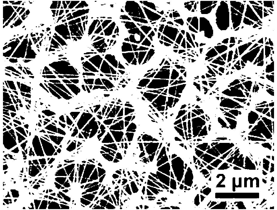
[0044] The difference between this example and Example 1 is that the one-dimensional tungsten oxide nanowire structure prepared in step (3) was prepared after a constant temperature of 1100 ° C for 60 minutes, and the prepared porous silicon-based one-dimensional tungsten oxide nanowire gas sensor 2ppmNO at 100℃ 2 Gas has a sensitivity of 3.05.

Embodiment 3

[0046] The difference between this example and Example 1 is that the one-dimensional tungsten oxide nanowires prepared in step (3) are prepared after a constant temperature of 1150° C. for 90 minutes, and the prepared porous silicon-based one-dimensional tungsten oxide nanowire gas sensor is 100℃ condition to 2ppm NO 2 Gas has a sensitivity of 2.51.


PUM

PropertyMeasurementUnit
Average pore sizeaaaaaaaaaa
Thicknessaaaaaaaaaa
Diameteraaaaaaaaaa

Abstract

The invention discloses a method for a preparing porous silicon-based one-dimensional nanowire gas sensitive element, wherein a silicon-based porous silicon composite one-dimensional tungsten oxide nano-structure which has the bore diameter in the range from 1 to 2 microns and also has highly orderly arranged ducts is taken as a gas sensitive element for the first time; due to huge specific surface area and high surface activity, lots of gas absorption positions and gas dispersion channels can be provided so that the gas sensitive element is easy to react with gas. The gas sensitive sensor element provided by the invention has high response value and good sensitivity and selectivity for low-concentration oxynitride gas at a low temperature (100 DEG C), and further is small in size, simple in structure, mature in fabrication process, convenient to use and low in price; as a result, the gas sensitive sensor element is expected to be popularized and applied to the field of the gas sensitive sensor.

Description

technical field [0001] The invention relates to a gas sensor, in particular to a method for preparing a micron-sized porous silicon-based one-dimensional tungsten oxide nanostructure gas sensor that can work at a lower temperature and is suitable for detecting nitrogen oxide gas. Background technique [0002] With the rapid development of industrial technology and the continuous improvement of people's living standards, various gas pollutants brought about in the process of production and life have increased significantly. Nitrogen oxides (NO x ) as a highly toxic gas is the main source of acid rain and photochemical smog, which has posed a serious threat to human health and safety. Therefore, the detection of nitrogen oxide gas has become a research hotspot in recent years. In recent years, with the continuous development of nanotechnology, nanostructured gas sensor devices have achieved considerable development. Especially in order to meet the urgent needs of industrial ...

Claims


Application Information

Patent Timeline
IPC IPC(8): G01N27/00C23C16/40C25F3/12C23C14/35B82Y15/00B82Y30/00
Inventor 胡明马双云曾鹏李明达闫文君
Owner TIANJIN UNIV
Why Eureka
Try Eureka