Semiconductor device connection high purity copper fine wire

A high-purity, semi-conductive technology, applied in the direction of semiconductor devices, semiconductor/solid-state device manufacturing, electrical solid-state devices, etc., can solve problems such as impossibility to prevent oxygen penetration

Active Publication Date: 2013-09-04
TANAKA DENSHI KOGYO KK
View PDF8 Cites 4 Cited by
  • Summary
  • Abstract
  • Description
  • Claims
  • Application Information

AI Technical Summary

Problems solved by technology

However, thin noble metal layers are not free of cracks, pinholes, etc. in them, and during the high temperature final heat treatment, it has been expected to be impossible to prevent the penetration

Method used


Image

  • Semiconductor device connection high purity copper fine wire
  • Semiconductor device connection high purity copper fine wire
  • Semiconductor device connection high purity copper fine wire

Examples


Embodiment 1

[0063] {Example 1}

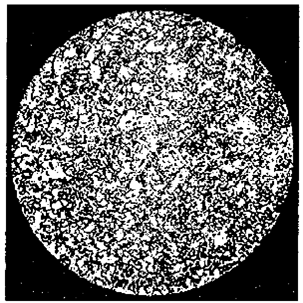
[0064] The oxide layer of a copper fine wire preform having a diameter of 2 mm and made of copper with a purity of 99.99992% by mass consists of a 0.5-nm-thick outermost layer of copper dioxide and a 3-nm-thick sublayer of copper monoxide constitute. The preformed copper thin wire is continuously drawn to obtain a copper thin wire with a diameter of 0.2 mm (reference figure 1 ). as in figure 1 As clearly seen in the cross-sectional photographs of , even after a low-temperature heat treatment at 500 °C, there is still a microtexture in the copper matrix induced by wire drawing.

[0065] This thin copper wire was run at a speed of 100m / min through a vertical heat treatment furnace (700°C reading; length 50cm) with a forming gas atmosphere containing 5% hydrogen and 95% nitrogen, and in pure water at 20°C Cool in medium. After water cooling, it is wound on a bobbin; the oxide film of the high-purity copper fine wire has been thinned, and it consists of a...

Embodiment 2

[0072] {Example 2}

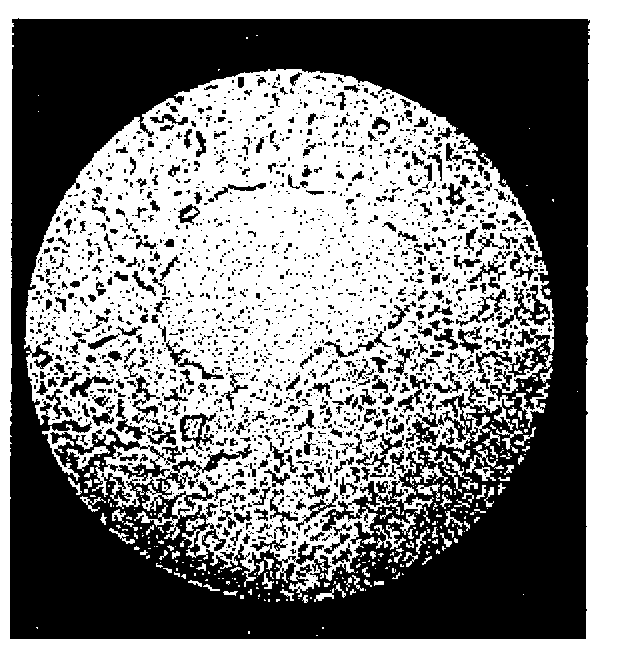
[0073] The oxide layer of a copper thin wire preform having a diameter of 5 mm and made of penta-nine-pure copper containing 20 mass ppm of silver, 2 mass ppm of iron and the balance of 99.9997 mass % of copper has a 0.5-nm- A thick outermost layer of copper dioxide and a 4-nm-thick sublayer of copper monoxide, similar to the fine wire preform of Example 1. This copper fine wire preform was continuously drawn to obtain a copper fine wire with a diameter of 0.5 mm. The cross-sectional structure of this thin copper wire is roughly similar to that in Figure 4 The cross-sectional structure shown in .

[0074] The thin copper wire was run at a speed of 50 m / min through a red hot (about 800°C) vertical heat treatment furnace (length 100 cm) containing a nitrogen atmosphere and cooled in pure water at 30°C. After water cooling, it was wound on a bobbin; similarly to the case of Example 1, the oxide film of the high-purity copper thin wire composed of a copper...

Embodiment 3

[0076] {Example 3}

[0077] Copper fine wire with a diameter of 5 mm and made of copper containing 5 mass ppm silver, 5 mass ppm iron, 2 mass ppm nickel, 5 mass ppm silicon, 10 mass ppm phosphorus, and the balance 99.9997 mass % copper The oxide layer of the preform had a 0.5-nm-thick outermost layer of copper dioxide and a 5-nm-thick copper monoxide sublayer. This copper fine wire preform was continuously drawn to obtain a copper fine wire with a diameter of 0.5 mm. The cross-sectional structure of this thin copper wire is roughly similar to that in Figure 4 The cross-sectional structure shown in .

[0078] The thin copper wire was run at a speed of 50 m / min through a red hot (about 800°C) vertical heat treatment furnace (length 100 cm) containing a nitrogen atmosphere and cooled in pure water at 30°C. After water cooling, it was wound on a bobbin; the oxide film of the high-purity copper thin wire composed of a copper dioxide layer and a copper monoxide layer was as thin...


PUM

PropertyMeasurementUnit
Thicknessaaaaaaaaaa
Diameteraaaaaaaaaa
Diameteraaaaaaaaaa

Abstract

To provide high purity copper wire, particularly of sub-millimeter diameter, with which, by making a dual layer structure in a cross-section configuration of the high purity copper fine wire, mechanical strength is increased, and which is optimal for high-temperature power semiconductors in which on-off cycles are repeated over multiple iterations in a short time. The present invention relates to high purity copper fine wire which is contiguously extended for connecting a semiconductor device and which is formed from copper of a purity of 99.997mass%-99.99994mass% having an oxide film, in which the area of the top 10 grains in a cross-section configuration of the high purity copper fine wire is 5-25% of the total cross-section configuration, and 80% or more of the grain area is within a surface skin layer which is defined as 1/20 or less of the diameter. The high purity copper fine wire is prepared by continuously pulling and is used for connecting the semiconductor device.

Description

technical field [0001] The present invention relates to thin high-purity copper wires for connecting electrodes on semiconductor devices to external electrodes, and more particularly, to thin high-purity copper wires having enhanced texture and sub-micron diameters, and Made of a copper-based alloy formed by doping copper (Cu) with a purity of 99.9999% by mass with a very small amount of silver (Ag). Background technique [0002] Bonding pads are mounted on semiconductor devices made of materials such as silicon (Si), silicon carbide (SiC), and gallium nitride (GaN), and can be made of aluminum (Al), aluminum-based Alloys such as aluminum-plus-1-mass% silicon alloys, copper, nickel (Ni), silver, and platinum (Pt) are used to form substrates. Such a substrate may be coated with noble metals such as gold (Au) and silver by wet plating or dry plating such as magnetron sputtering and vapor deposition, or may be plated with nickel. In this specification, unless otherwise specif...

Claims


Application Information

Patent Timeline
IPC IPC(8): H01L21/60
CPCC22C9/00C22F1/08H01L24/05H01L24/43H01L24/45H01L24/48H01L24/85H01L2224/05624H01L2224/05644H01L2224/05647H01L2224/05655H01L2224/43H01L2224/4321H01L2224/43848H01L2224/45014H01L2224/45015H01L2224/45147H01L2224/45565H01L2224/45639H01L2224/45664H01L2224/48824H01L2224/48844H01L2224/48847H01L2224/48855H01L2224/85065H01L2224/85075H01L2224/85205H01L2924/00011H01L2924/00014H01L2924/01006H01L2924/01015H01L2924/01047H01L2924/10253H01L2924/10272H01L2924/1033H01L2924/15747H01L2924/01204H01L2924/01206H01L2924/01046H01L2924/01026H01L2924/01028H01L2924/0105H01L2924/01014H01L2924/01016H01L2924/00H01L2924/013H01L2224/48H01L2924/0002H01L2924/20752H01L2924/20756H01L2924/01205H01L2924/01007H01L2924/20305H01L2924/2076H01L2924/00013H01L2924/20751H01L2924/20757H01L2924/20758H01L2924/20759H01L2924/01004H01L2924/01033H01L2924/206
Inventor 三上道孝合濑昌章中岛伸一郎三村利孝弥永幸弘市川司高田晃
Owner TANAKA DENSHI KOGYO KK
Why Eureka
Try Eureka