Method for preparing silicon-based high-mobility CMOS (complementary metal-oxide-semiconductor) provided with III-V/Ge channel

A high-mobility, silicon-based technology used in microelectronics to address misfit dislocations, unrealized integration, and unsatisfactory III-V or germanium material quality

Active Publication Date: 2013-11-13
INST OF SEMICONDUCTORS - CHINESE ACAD OF SCI
View PDF7 Cites 8 Cited by
  • Summary
  • Abstract
  • Description
  • Claims
  • Application Information

AI Technical Summary

Problems solved by technology

Another solution to solve the III-V N-type channel and germanium P-type channel is to use silicon-based selective epitaxy, but the quality of III-V or germanium materials obtained by selective epitaxy is not ideal (micron size), The possibility of realizing this scheme remains to be investigated; at the same time, the extremely small-sized selected area epitaxy has gained great attention in recent years through the high aspect ratio trapping (ART) (J.S.Park et al, Appl.Phys.Lett.90, 052113, 2007), in the SiO2 trench, the epitaxial material is grown along the crystal plane (parallel to the trench direction) composed of {311} and {111} crystal groups, and the misalignment at the Si-Ge interface Misalignment defects generally extend along the growth direction of the epitaxial layer
However, the integration of silicon-based high-mobility N and P channels through this scheme has not yet been realized.

Method used


Image

  • Method for preparing silicon-based high-mobility CMOS (complementary metal-oxide-semiconductor) provided with III-V/Ge channel
  • Method for preparing silicon-based high-mobility CMOS (complementary metal-oxide-semiconductor) provided with III-V/Ge channel
  • Method for preparing silicon-based high-mobility CMOS (complementary metal-oxide-semiconductor) provided with III-V/Ge channel

Examples


Embodiment Construction

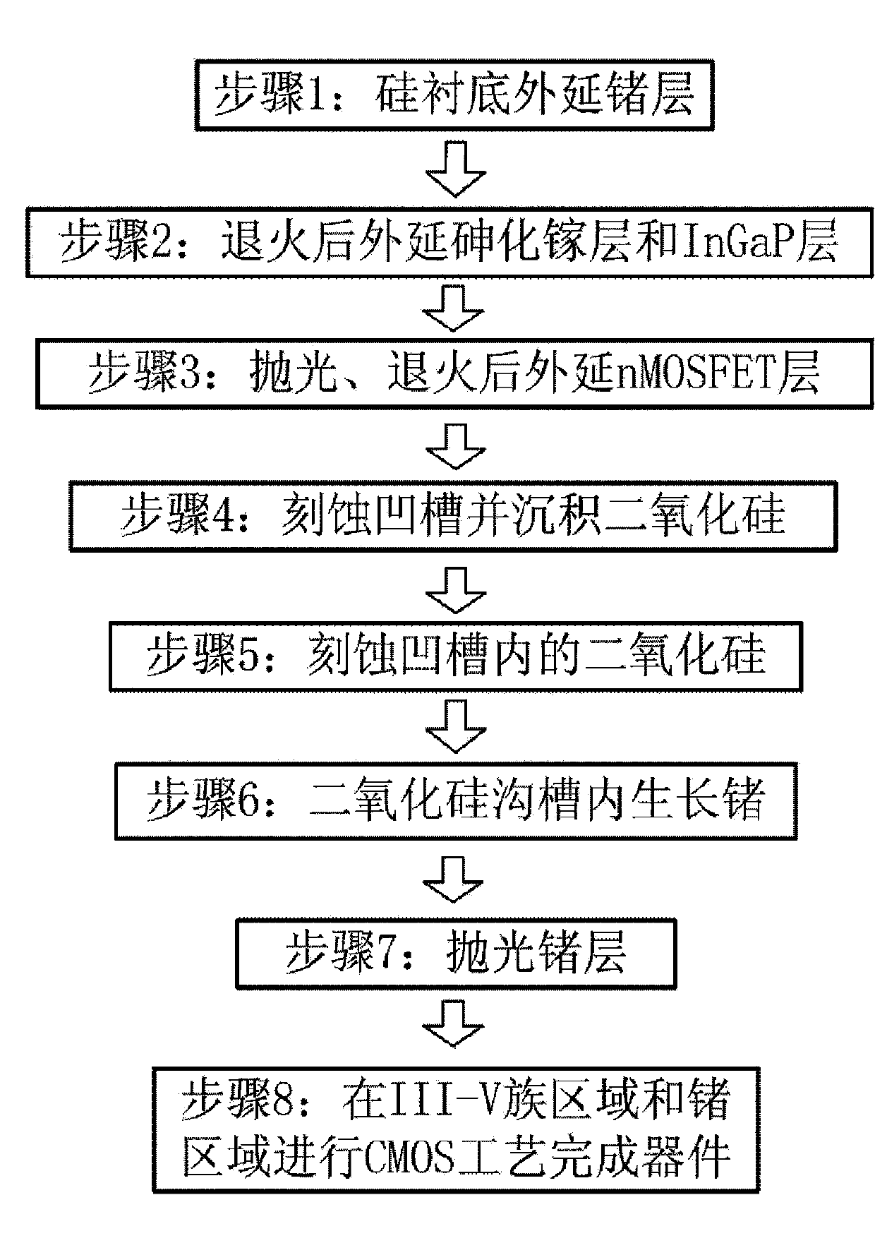
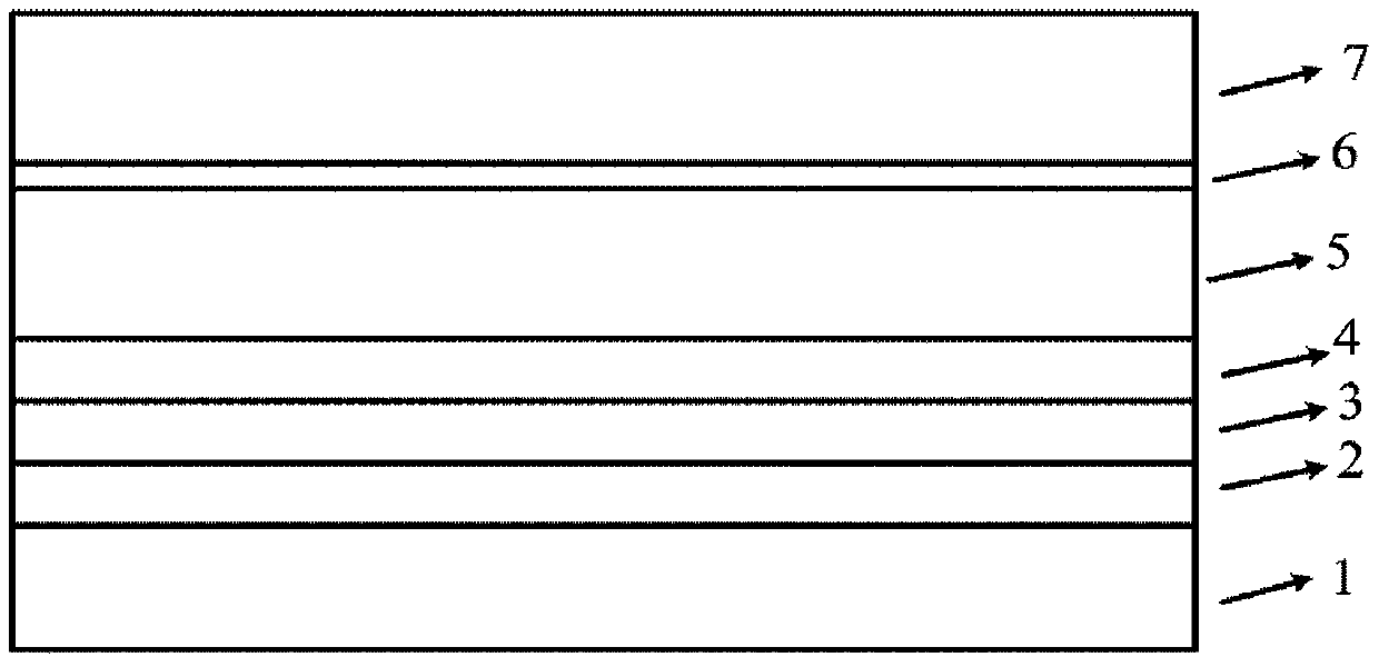
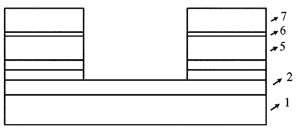
[0024] see figure 1 and refer to Figure 2 to Figure 9 , the invention provides a CMOS preparation method of a silicon-based high-mobility III-V / Ge channel, comprising the following steps:

[0025] Step 1: On the cleaned silicon substrate 1, a germanium layer 2 is grown by ultra-high vacuum chemical vapor deposition (see figure 2 ). The silicon substrate 1 is a (100) substrate that is 4° off the [011] direction. The substrate off-angle is to ensure that atomic steps are formed on the surface of the final germanium layer to suppress the reverse domain when gallium arsenide is nucleated. The off angle is generally 3° to 6°; the transition of the lattice constant to gallium arsenide is realized through the germanium layer, and the defect density of the germanium layer needs to be 1×10 6 cm -2 Below, the surface roughness RMS is less than 0.5 nm.

[0026] Step 2: Put the silicon substrate 1 into the MOCVD reaction chamber immediately, after the first annealing, grow the low-...


PUM

PropertyMeasurementUnit
thicknessaaaaaaaaaa
widthaaaaaaaaaa
surface roughnessaaaaaaaaaa

Abstract

The invention discloses a method for preparing a silicon-based high-mobility CMOS provided with an III-V/Ge channel. The method comprises steps as follows: a germanium layer is grown on a silicon substrate; a low-temperature nucleation gallium arsenide layer, a high-temperature gallium arsenide layer, an on-growth semi-insulating InGaP (gallium indium phosphide) layer and a gallium arsenide cover coating are sequentially grown on the germanium layer after the first annealing, so that a sample is formed; the gallium arsenide cover coating of the sample is subjected to a gallium arsenide polishing process, and a nMOSFET (metal oxide semiconductor field effect transistor) structure is grown after the sample is subjected to secondary annealing; an area is selected on the surface of the nMOSFET structure for ICP (inductively coupled plasma) etching, downward etching from the nMOSFET structure to the germanium layer is performed to form a groove, and silicon dioxide layers are grown in the groove and on the surface of the nMOSFET structure in a PECVD (plasma enhanced chemical vapor deposition) manner; the area selected for etching is subjected to ICP etching again from the silicon dioxide layers to the germanium layer, and a groove is formed; the sample is cleaned, and a germanium nucleating layer and a germanium top layer are grown in the groove with an ultra-high vacuum chemical vapor deposition method; the germanium top layer is polished, and a part of silicon dioxide layers on the nMOSFET structure are removed; and the CMOS process of source, drain and grid electrodes is performed on the nMOSFET structure and the germanium top layer, so that the preparation of the device is finished.

Description

technical field [0001] The invention relates to the field of microelectronics, combines ultra-high vacuum chemical vapor deposition with MOCVD, and uses high aspect ratio confinement technology to realize simultaneous integration of silicon-based high-mobility III-V / Ge channel materials, and is applied to silicon-based III-V / Ge channel CMOS devices. Background technique [0002] The feature size drops to 22nm node, and the integrated circuit technology based on silicon CMOS technology follows Moore's law to achieve the purpose of increasing the working speed of the chip, increasing the integration level and reducing the cost by reducing the feature size of the device, and difficulties have arisen. Factors such as the increase in the cost of the nanofabrication process, the short-channel effect that reduces the gate control capability, and the limitation of the mobility of the silicon material itself negate the possibility of continuing to shrink the feature size of the devi...

Claims


Application Information

Patent Timeline
Patent Type & Authority Applications(China)
IPC IPC(8): H01L21/8258
CPCH01L21/02381H01L21/02433H01L21/0245H01L21/02461H01L21/02463H01L21/02505H01L21/02546H01L21/0262H01L21/8258H01L27/0605
Inventor 周旭亮于红艳李士颜潘教青王圩
Owner INST OF SEMICONDUCTORS - CHINESE ACAD OF SCI
Why Eureka
Try Eureka