Method for manufacturing multi-wavelength photonic integration transmitter chip through quantum well intermixing

A quantum well hybrid, photon integration technology, applied in phonon exciters, lasers, laser components, etc., can solve problems such as lattice damage in quantum well regions, increased waveguide loss, and active integration limitations.

Active Publication Date: 2013-11-27
INST OF SEMICONDUCTORS - CHINESE ACAD OF SCI
View PDF5 Cites 15 Cited by
  • Summary
  • Abstract
  • Description
  • Claims
  • Application Information

AI Technical Summary

Problems solved by technology

The technology of introducing defects through phosphorus ion implantation to achieve quantum well hybridization has been applied to 1nP-based photonic integrated devices, but the phosphorus ion implantation method will cause damage to the lattice of the quantum well region and increase waveguide loss, which is limited in active integration. limit

Method used


Image

  • Method for manufacturing multi-wavelength photonic integration transmitter chip through quantum well intermixing
  • Method for manufacturing multi-wavelength photonic integration transmitter chip through quantum well intermixing
  • Method for manufacturing multi-wavelength photonic integration transmitter chip through quantum well intermixing

Examples


Embodiment 1

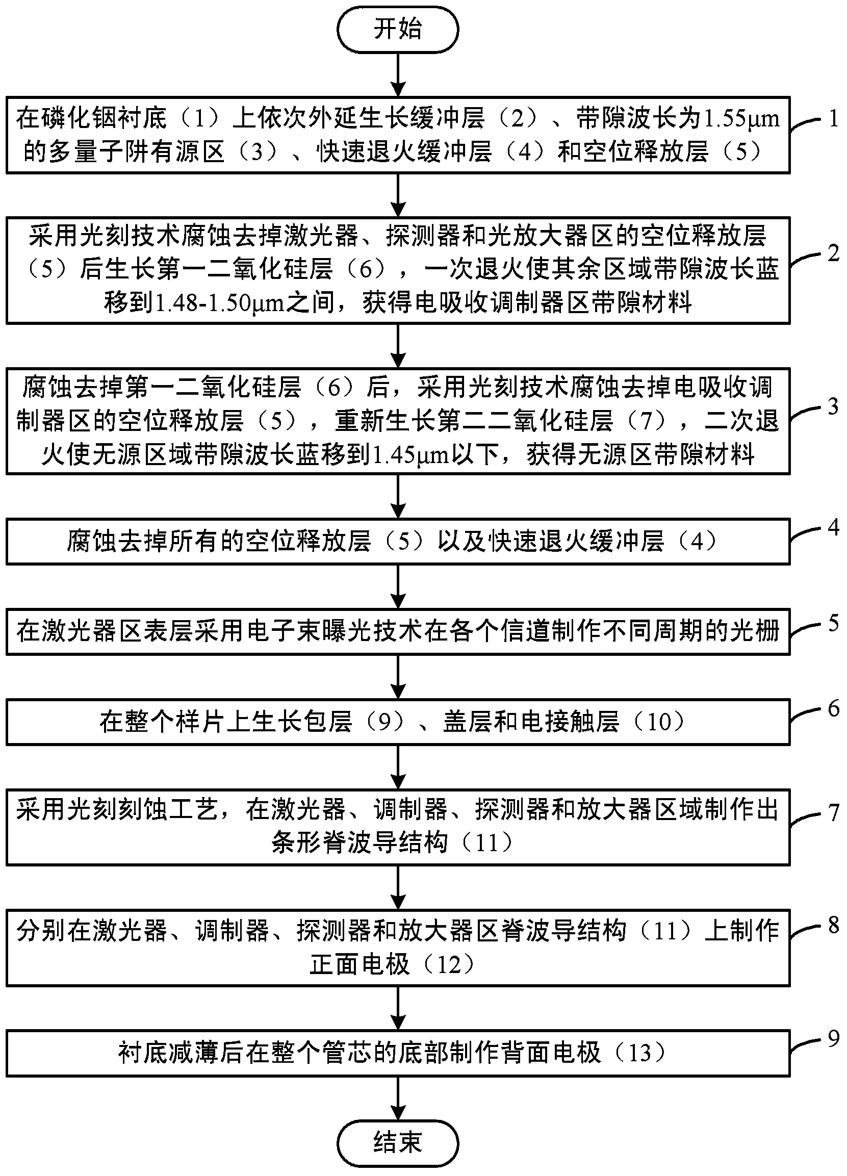
[0058] In a preferred embodiment of the present invention, described a kind of method utilizing quantum well hybridization to make multi-wavelength photon integrated emitter chip comprises the following steps:

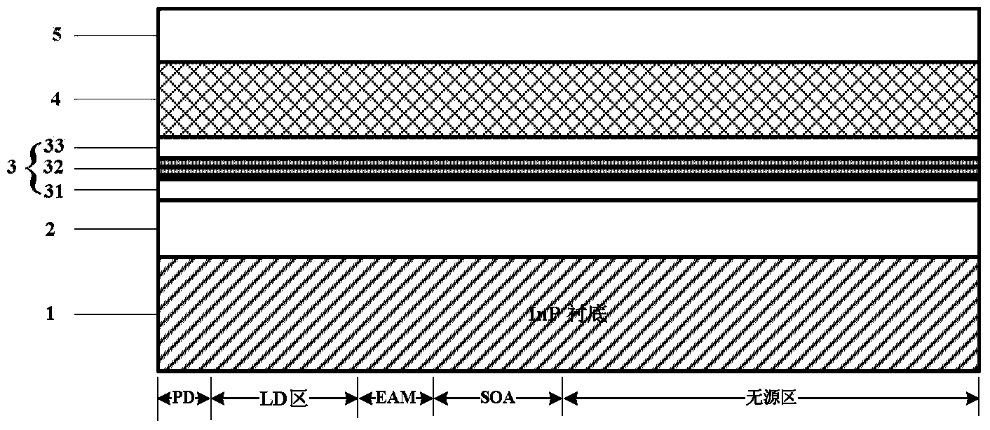
[0059] At a doping concentration of 5×10 17 cm -3 On an indium phosphide substrate 1, a buffer layer 2, a multi-quantum well active region 3 with a bandgap wavelength of 1.55 μm, a rapid annealing buffer layer 4 with a thickness of 300 nm, and a vacancy release layer 5 with a thickness of 300 nm are sequentially grown on an indium phosphide substrate. The quantum well active region 3 includes a lower waveguide layer 31 , a core layer 32 and an upper waveguide layer 33 grown sequentially.

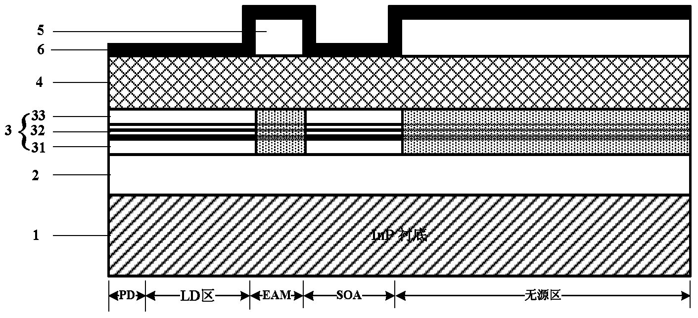
[0060] Using conventional photolithography technology, etch and remove the vacancy release layer 5 in the laser, detector and optical amplifier area, then use PECVD to grow a layer of silicon dioxide 6 with a thickness of 150nm, and anneal once at 670°C under the annealing condition...

Embodiment 2

[0065] At a doping concentration of 5×10 18 cm -3 On an indium phosphide substrate 1, a buffer layer 2, a multi-quantum well active region 3 with a bandgap wavelength of 1.55 μm, a rapid annealing buffer layer 4 with a thickness of 500 nm, and a vacancy release layer 5 with a thickness of 450 nm are grown sequentially on an indium phosphide substrate. The quantum well active region 3 includes a lower waveguide layer 31 , a core layer 32 and an upper waveguide layer 33 grown sequentially.

[0066] Using conventional photolithography technology, etch away the vacancy release layer 5 in the laser, detector and optical amplifier area, then use PECVD to grow a layer of silicon dioxide 6 with a thickness of 250nm, and anneal once at 685°C under the annealing conditions of 120s to make the band gap in the remaining areas The wavelength is blue-shifted to 1.48 μm, and the bandgap material of the electroabsorption modulator region is obtained, in which the lengths of the laser, detect...

Embodiment 3

[0071] In another preferred embodiment of the present invention, described a kind of method utilizing quantum well hybridization to make multi-wavelength photonic integrated emitter chip comprises the following steps:

[0072] At a doping concentration of 1×10 18 cm -3 On an indium phosphide substrate 1, a buffer layer 2, a multi-quantum well active region 3 with a bandgap wavelength of 1.55 μm, a rapid annealing buffer layer 4 with a thickness of 400 nm, and a vacancy release layer 5 with a thickness of 400 nm are grown sequentially on an indium phosphide substrate. The quantum well active region 3 includes a lower waveguide layer 31 , a core layer 32 and an upper waveguide layer 33 grown sequentially.

[0073] Using conventional photolithography technology, etch and remove the vacancy release layer 5 in the laser, detector and optical amplifier area, then use PECVD to grow a layer of silicon dioxide 6 with a thickness of 200nm, and anneal once at 678°C under the annealing c...


PUM


Abstract

The invention discloses a method for manufacturing a multi-wavelength photonic integration transmitter chip through quantum well intermixing. The method comprises the followings steps: sequentially manufacturing a buffer layer, a multiple-quantum-well active region, a rapid annealing buffer layer and a vacancy releasing layer on a substrate in an extension mode, conducting corrosion to remove vacancy releasing layers on a laser region, a detector region and a light amplifier region, then growing silicon dioxide, conducting first-time annealing to obtain electric absorption modulator region materials, conducting corrosion to remove a vacancy releasing layer on an electric absorption modulator region, conducting second-time annealing to obtain passive region materials, conducting corrosion to remove all vacancy releasing layers and all rapid annealing buffer layers, manufacturing optical gratings on the surface layer of the laser region, growing a cover layer and an electric contact layer, then manufacturing the strip-type ridge waveguide, respectively manufacturing a front face electrode and a back face electrode on an active region ridge waveguide structure and the thinned substrate, and completing manufacturing of the tube chip. The manufacturing of the whole photonic integration transmitter chip only requires two extension steps, then integration between active region materials with different band gaps and passive region materials with different band gaps can be completed, the cost is low, the yield is high, and the method is suitable for popularization.

Description

technical field [0001] The invention relates to the field of optoelectronic devices, in particular to a method for manufacturing a multi-wavelength photon integrated emitter chip by using quantum well hybridization. Background technique [0002] Optical communication systems and networks have become an irreplaceable information-carrying platform in the national information infrastructure and an indispensable part of people's lives and work. Among them, photonic integrated circuits (PIC) is a technology that must be relied on to realize large-capacity, low-power optical networks in the future, and multi-wavelength photonic integrated chips will become the core of high-speed data transmission. For the multi-wavelength photonic integrated emitter chip with high integration and complex process preparation, because it contains functional devices with three bandgap wavelengths: DFB laser, SOA optical amplifier and PD detector (1.55 μm), EAM electroabsorption modulator ( 1.48-1.50...

Claims


Application Information

Patent Timeline
Patent Type & Authority Applications(China)
IPC IPC(8): H01S5/343
Inventor 张灿朱洪亮梁松
Owner INST OF SEMICONDUCTORS - CHINESE ACAD OF SCI
Why Eureka
Try Eureka