
Preparation method of a ternary (sb1-xbix)2se3 nanowire with adjustable composition

A sb1-xbix and nanowire technology, applied in the field of material science, can solve problems such as low spectral responsivity, many nanowire defects, and poor crystallization, and achieve the effects of simple preparation process, convenient regulation, and easy regulation of reaction conditions

Active Publication Date: 2016-04-27
SUZHOU INST OF NANO TECH & NANO BIONICS CHINESE ACEDEMY OF SCI
View PDF5 Cites 2 Cited by
  • Summary
  • Abstract
  • Description
  • Claims
  • Application Information

AI Technical Summary

Problems solved by technology

[0003] Sb 2 Se 3 The material is a semiconductor material with a band gap of about 1.2eV, which has great potential for red light detection applications, but currently Sb is usually prepared by hydrothermal method or template method. 2 Se 3 Nanowire structure with very low spectral responsivity R λ (8.0A / W) and external quantum effect EQE (1650%), which may be caused by the inherent defects such as many defects and poor crystallization of the nanowires prepared by the hydrothermal method

Method used


Image

  • Preparation method of a ternary (sb1-xbix)2se3 nanowire with adjustable composition

Examples


preparation example Construction

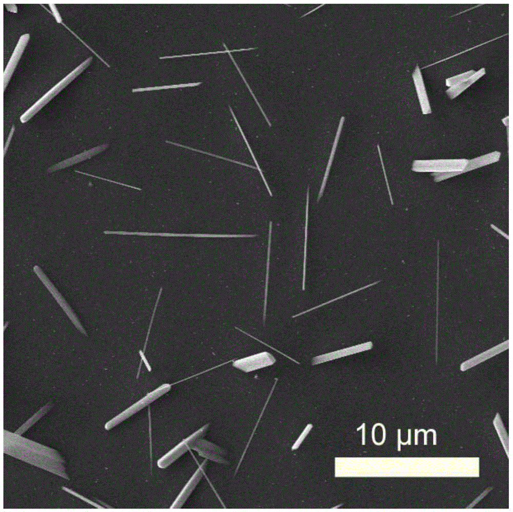
[0027] In a typical embodiment of the present invention, the preparation method comprises: firstly Sb 2 Se 3 Powder and Bi 2 Se 3 The powder is mixed in a certain proportion as the growth source and placed in the center of the quartz tube of the tube furnace for chemical vapor deposition. The silicon wafer with gold particles is placed at the downstream position of the quartz tube airflow and the quartz tube is sealed; the quartz tube is sealed with a mechanical pump. Exhaust the oxygen in the tube as much as possible, then fill it with a certain flow rate of high-purity argon as a carrier gas, and combine with the vacuum mechanical pump to maintain a certain vacuum degree in the quartz tube; react at a certain temperature for a period of time; after the reaction is completed, it can be cooled at room temperature get (Sb 1-x Bi x ) 2 Se 3 Nanowires (x=0~0.88). This method uses a simple chemical vapor deposition method, and by changing the ratio of growth sources or grow...

Embodiment 1

[0040] (1) Preparation of silicon wafers with colloidal gold particles: Submerge the silicon wafers with acetone, ethanol and deionized water for 10 minutes, and then dry them with nitrogen; immerse the cleaned silicon wafers in 0.1wt% poly-L- Lysine aqueous solution for 1 minute, then rinse with deionized water to positively charge the surface of the silicon wafer; then immerse the silicon wafer in a colloidal gold liquid with a diameter of 10nm for 1 minute, then rinse with deionized water, and finally blow dry with nitrogen , to obtain a silicon wafer with gold particles attached to the surface;

[0041] (2) Sb with a mass of 10 mg 2 Se 3 The powder is placed in the center of the quartz tube; the silicon wafer with gold particles attached is placed at the downstream position of the quartz tube airflow and the quartz tube is sealed; the inner chamber of the quartz tube is pumped and filtered to below 10mTorr with a mechanical pump, and then filled with an appropriate amount...

Embodiment 2

[0045] (1) Preparation of silicon wafers with colloidal gold particles: Submerge the silicon wafers with acetone, ethanol and deionized water for 10 minutes, and then dry them with nitrogen; immerse the cleaned silicon wafers in 0.1wt% poly-L Acid solution for 1 minute, then rinse with deionized water to make the surface of the silicon wafer positively charged; then immerse the silicon wafer in a colloidal gold liquid with a diameter of 10nm for 1 minute, then rinse with deionized water, and finally blow dry with nitrogen. Obtain a silicon wafer with gold particles attached to the surface;

[0046] (2) Sb with a mass of 7.5mg 2 Se 3 Powder with 2.5mg of Bi 2 Se 3 The powder is mixed and placed in the center of the quartz tube; the silicon wafer with gold particles attached is placed at the downstream position of the quartz tube airflow and the quartz tube is sealed; the inner chamber of the quartz tube is pumped and filtered to below 10mTorr with a mechanical pump, and then...


PUM

PropertyMeasurementUnit
diameteraaaaaaaaaa
lengthaaaaaaaaaa

Abstract

The invention discloses a method for preparing (Sb1-xBix)2Se3 nanowires with adjustable composition, including: (1) providing a substrate with colloidal gold particles attached to the surface and a growth source mainly formed by mixing Sb2Se3 powder and Bi2Se3 powder; ( 2) placing both the substrate and the growth source in the reaction area of ​​the chemical vapor deposition equipment, and setting the substrate downstream of the growth source, and then sealing the reaction area; (3) excluding the reaction area Oxygen in the interior, and then input rare gas as carrier gas, and the air pressure of described reaction area is all maintained in setting range, and adjusts reaction temperature to set value, until reaction is finished, then cools to room temperature, obtains (Sb1-xBix ) 2Se3 nanowires, wherein x=0~0.88. The present invention uses a simple chemical vapor deposition method, by changing the ratio of the growth source or the growth temperature, to obtain a single crystal (Sb1-xBix)2Se3 nanowire with adjustable composition and high quality, which can be used as a properties of new photodetector materials for a wide range of applications.

Description

technical field [0001] The invention relates to a preparation method of a photoelectric detection material, in particular to a composition-adjustable (Sb 1-x Bi x ) 2 Se 3 The invention relates to a method for preparing nanowires, belonging to the field of material science. Background technique [0002] Photodetection refers to the physical phenomenon of a change in the electrical conductivity of a material caused by radiation. Photodetectors can be used in optical detectors, photometry, infrared remote sensing, missile guidance, and can also be used in inductively coupled devices to record images in astronomy or digital photography, etc. [0003] Sb 2 Se 3 The material is a semiconductor material with a band gap of about 1.2eV, which has great potential for red light detection applications, but currently Sb is usually prepared by hydrothermal method or template method. 2 Se 3 Nanowire structure with very low spectral responsivity R λ (8.0A / W) and external quantum e...

Claims


Application Information

Patent Timeline
Patent Type & Authority Patents(China)
IPC IPC(8): C30B25/02C30B29/46C30B29/62B82Y40/00
Inventor 程国胜黄荣孔涛卫芬芬张杰
Owner SUZHOU INST OF NANO TECH & NANO BIONICS CHINESE ACEDEMY OF SCI
Learn More