IGZO (indium gallium zinc oxide) thin film transistor and preparing method thereof

A thin film transistor and film layer technology, applied in the field of microelectronics, can solve the problems of reducing the electrical performance of the device and affecting the charge transfer in the device, and achieve the effects of low cost, easy control of conditions and high mobility

Active Publication Date: 2014-04-02
TCL CORPORATION
View PDF3 Cites 25 Cited by
  • Summary
  • Abstract
  • Description
  • Claims
  • Application Information

AI Technical Summary

Problems solved by technology

[0006] The purpose of the present invention is to overcome the above-mentioned deficiencies of the prior art, and to provide an IGZO thin film transistor, which aims to solve the problem that there are traps and defects at the interface

Method used


Image

  • IGZO (indium gallium zinc oxide) thin film transistor and preparing method thereof
  • IGZO (indium gallium zinc oxide) thin film transistor and preparing method thereof
  • IGZO (indium gallium zinc oxide) thin film transistor and preparing method thereof

Examples


preparation example Construction

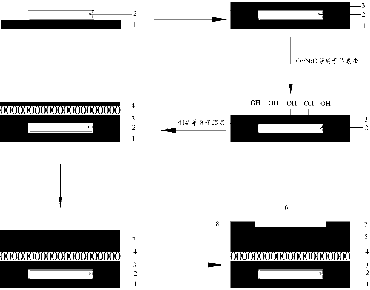
[0030] Correspondingly, a method for preparing an IGZO thin film transistor with high mobility and excellent device performance comprises the following steps:

[0031] S01. Covering the outer surface of the substrate 1 combined with the gate 2 and the outer surface of the gate 2 with silicide to form a silicide gate insulating layer 3;

[0032] S02. Use O 2 / N 2 O plasma bombards the silicide gate insulating layer 3 to obtain a modified silicide gate insulating layer;

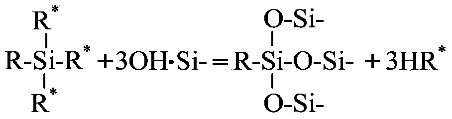
[0033] S03. Prepare a self-assembled monomolecular film layer 4 on the outer surface of the modified silicide gate insulating layer;

[0034] S04. Prepare an IGZO active layer 5 on the outer surface of the self-assembled monomolecular film layer 4, and prepare an etching stopper layer 6, a source electrode 7 and a drain electrode 8 on the IGZO active layer 5 to obtain a prepared IGZO thin film transistor, Afterwards, it is annealed to obtain the above-mentioned IGZO thin film transistor.

[0035] The proces...

Embodiment 1

[0048] A preparation method for an IGZO thin film transistor, comprising the steps of:

[0049] S11. Using a heavily doped N-type silicon wafer as a substrate, prepare a silicide gate insulating layer on the heavily doped N-type silicon wafer substrate by a thermal oxidation method, and then use HF to clean the back side of the insulating layer;

[0050] S121. First take the absorbent cotton ball dipped in acetone and repeatedly scrub the silicide gate insulating layer to erase the pollutants left on the surface of the silicide gate insulating layer; then clean the entire substrate combined with the silicide gate insulating layer with Cleaning solution, acetone, isopropanol and deionized water were ultrasonically cleaned for 20 minutes, and dried in an oven to obtain a clean and dry heavily doped N-type silicon wafer substrate with a silicide gate insulating layer;

[0051]S122. Adopt PECVD equipment, set the air pressure in the cavity to 200mtorr, and process for 3 minutes, O...

Embodiment 2

[0059] A kind of preparation method of IGZO thin film transistor, its concrete steps are similar to embodiment 1, difference is: the O 2 The flow rate is 100 sccm, and the processing time is 1.5 minutes; when self-assembling a monomolecular film layer at the same time, the silane mixed solution is prepared from phenylethyltrichlorosilane and a mixed solvent composed of chloroform and cyclohexane with a volume ratio of 3:7 , and the concentration is 5mg / ml, placed on a hot stage at 60°C, and the reaction time is 40 minutes. Specific steps are as follows:

[0060] S222. Adopt PECVD equipment, and set the air pressure in the chamber to be 200mtorr, the processing time is 1.5 minutes, O 2 The flow rate is 100sccm, the processing power is 40W, and the surface of the silicide gate insulating layer is O 2 Plasma bombardment.

[0061] S231. Prepare a mixed solvent of phenethyltrichlorosilane and chloroform and cyclohexane with a volume ratio of 3:7 to form a mixed solution with a c...


PUM

PropertyMeasurementUnit
Thicknessaaaaaaaaaa

Abstract

The invention discloses an IGZO (indium gallium zinc oxide) thin film transistor and a preparing method thereof, wherein the IGZO thin film transistor comprises a substrate, a grid combined on the substrate surface and a silicide grid insulation layer covering the outer surfaces of the substrate and the grid, wherein the surface of the silicide grid insulation layer is subjected to O2/N2O plasma bombardment processing; the surface of the silicide grid insulation layer subjected to the O2/N2O plasma bombardment processing is also combined with a self-assembly single-molecule film layer in a laminating mode, so the film defect state of the silicide grid insulation layer can be reduced after the O2/N2O plasma bombardment, the charge trap action is inhibited, the roughness of the surface of the insulation layer is reduced by the self-assembly single-molecule film layer, the interface property between the insulation layer and an active layer is well improved, charges are prevented from being captured by an interface defect, the carrier mobility of a device is reduced, the threshold voltage is reduced, leak current is reduced and the performance of the device is more stable.

Description

technical field [0001] The invention belongs to the technical field of microelectronics, and in particular relates to an IGZO thin film transistor and a preparation method thereof. Background technique [0002] The IGZO thin film transistor device structure commonly used at present is a bottom-gate top-contact structure, which includes a substrate, a gate, a gate insulating layer, an IGZO active layer, an etch stop layer, and a source-drain electrode from bottom to top. The insulating layer is mostly an inorganic insulating material, such as SiO 2 , SiNx, Al 2 o 3 、 Ta 2 o 5 Wait. The IGZO active layer is grown on the gate insulating layer, that is to say, the selection of the gate insulating layer material and the surface quality of the gate insulating layer film have a great influence on the device performance of the IGZO thin film transistor. [0003] As an important part of the IGZO thin film transistor, the gate insulating layer is made of SiO 2 more common. But...

Claims


Application Information

Patent Timeline
IPC IPC(8): H01L29/786H01L21/336
CPCH01L21/28264H01L29/513H01L29/66969H01L29/78693
Inventor 杨帆申智渊付东
Owner TCL CORPORATION
Why Eureka
Try Eureka