Photocatalytic material with visible light response capability and core-shell structure, and preparation method
A technology of photocatalytic material and core-shell structure, which is applied in the field of core-shell structure photocatalytic material and preparation, and can solve the problems of limited life of catalyst and weak structure stability.
- Summary
- Abstract
- Description
- Claims
- Application Information
AI Technical Summary
Problems solved by technology
Method used
Image
Examples
Embodiment 1
[0019] The first step is to prepare rod-shaped single crystal ZnO:
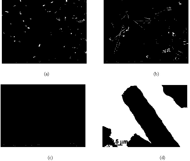
[0020] Mix ZnO and graphite powder with a mass ratio of 1:1 evenly, put them into a quartz boat, put the quartz boat into the middle of the horizontal tube furnace, and place the cleaned silicon wafer at the 5-10cm downwind end of the quartz boat Substrate, the silicon substrate adopts single crystal silicon wafer with crystal orientation, and heats the horizontal tube furnace for one hour to make ZnO undergo redox reaction. ~99.999% nitrogen is used as the carrier gas, the flow rate is controlled at 40~65sccm, and then cooled naturally, the product on the silicon wafer substrate is collected, and finally a pure white product of ZnO is obtained. The crystal structure of ZnO is shown in figure 1 In figure a in the middle, there is a rod-shaped single crystal with a length of 5-15 μm and a diameter of about 300-600 nm.
[0021] The second step V 2 o 5 Coating of precursor on ZnO surface:
[0022] Vanadyl a...
Embodiment 2
[0028] The first step is to prepare rod-shaped single crystal ZnO:
[0029]Mix ZnO and graphite powder with a mass ratio of 3:1 evenly, put it into a quartz boat, put the quartz boat into the middle of the horizontal tube furnace, and place the cleaned silicon wafer at the 5-10cm downwind end of the quartz boat The substrate, the substrate is made of silicon dioxide substrate, and the horizontal tube furnace is heated for 1.2 hours to make ZnO undergo oxidation-reduction reaction. Carrier gas, the flow rate is controlled at 40-65sccm, and then naturally cooled to collect the product on the silicon wafer substrate, and finally a pure white ZnO product is obtained. The crystal structure of ZnO is shown in figure 1 In figure a in the middle, there is a rod-shaped single crystal with a length of 5-15 μm and a diameter of about 300-600 nm.
[0030] The second step V 2 o 5 Coating of precursor on ZnO surface:
[0031] Use vanadyl acetylacetonate as the vanadium raw material, put...
Embodiment 3
[0036] The first step is to prepare rod-shaped single crystal ZnO:
[0037] In the first step, mix ZnO and graphite powder with a mass ratio of 5:1 evenly, put them into a quartz boat, then put the quartz boat into the middle of the horizontal tube furnace, and place a washing Clean silicon wafer substrate, the substrate is made of sapphire substrate, heated in a horizontal tube furnace for 0.8 hours to make ZnO undergo oxidation-reduction reaction, the heating temperature is controlled at about 900 ° C, and the purity is 98.5% ~ 99.999% Nitrogen is used as the carrier gas, the flow rate is controlled at 40-65 sccm, and then cooled naturally, the product on the silicon wafer substrate is collected, and finally a pure white product of ZnO is obtained. The crystal structure of ZnO is shown in figure 1 In figure a in the middle, there is a rod-shaped single crystal with a length of 5-15 μm and a diameter of about 300-600 nm.
[0038] The second step V 2 o 5 Coating of precurso...
PUM
| Property | Measurement | Unit |
|---|---|---|
| thickness | aaaaa | aaaaa |
| length | aaaaa | aaaaa |
| diameter | aaaaa | aaaaa |
Abstract
Description
Claims
Application Information
 - R&D
- Intellectual Property
- Life Sciences
- Materials
- Tech Scout
- Unparalleled Data Quality
- Higher Quality Content
- 60% Fewer Hallucinations
Browse by: Latest US Patents, China's latest patents, Technical Efficacy Thesaurus, Application Domain, Technology Topic, Popular Technical Reports.
© 2025 PatSnap. All rights reserved.Legal|Privacy policy|Modern Slavery Act Transparency Statement|Sitemap|About US| Contact US: help@patsnap.com


