Organic light-emitting device and preparation method thereof
An electroluminescent device and luminescent technology, which are applied in the manufacture of organic semiconductor devices, electric solid devices, semiconductor/solid state devices, etc., to achieve the effects of improving lifespan, easy large-scale preparation, and cheap materials
- Summary
- Abstract
- Description
- Claims
- Application Information
AI Technical Summary
Problems solved by technology
Method used
Image
Examples
preparation example Construction
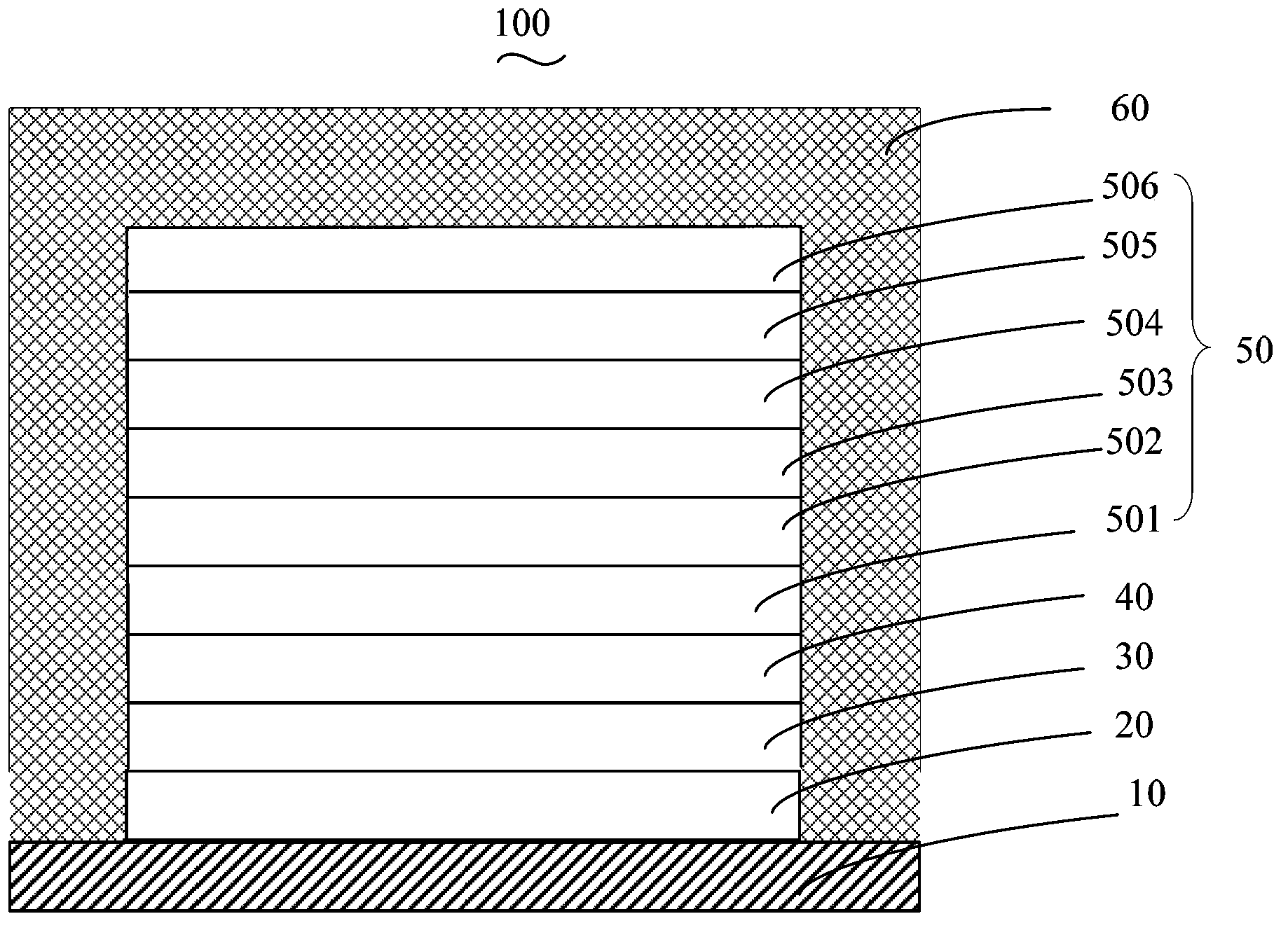
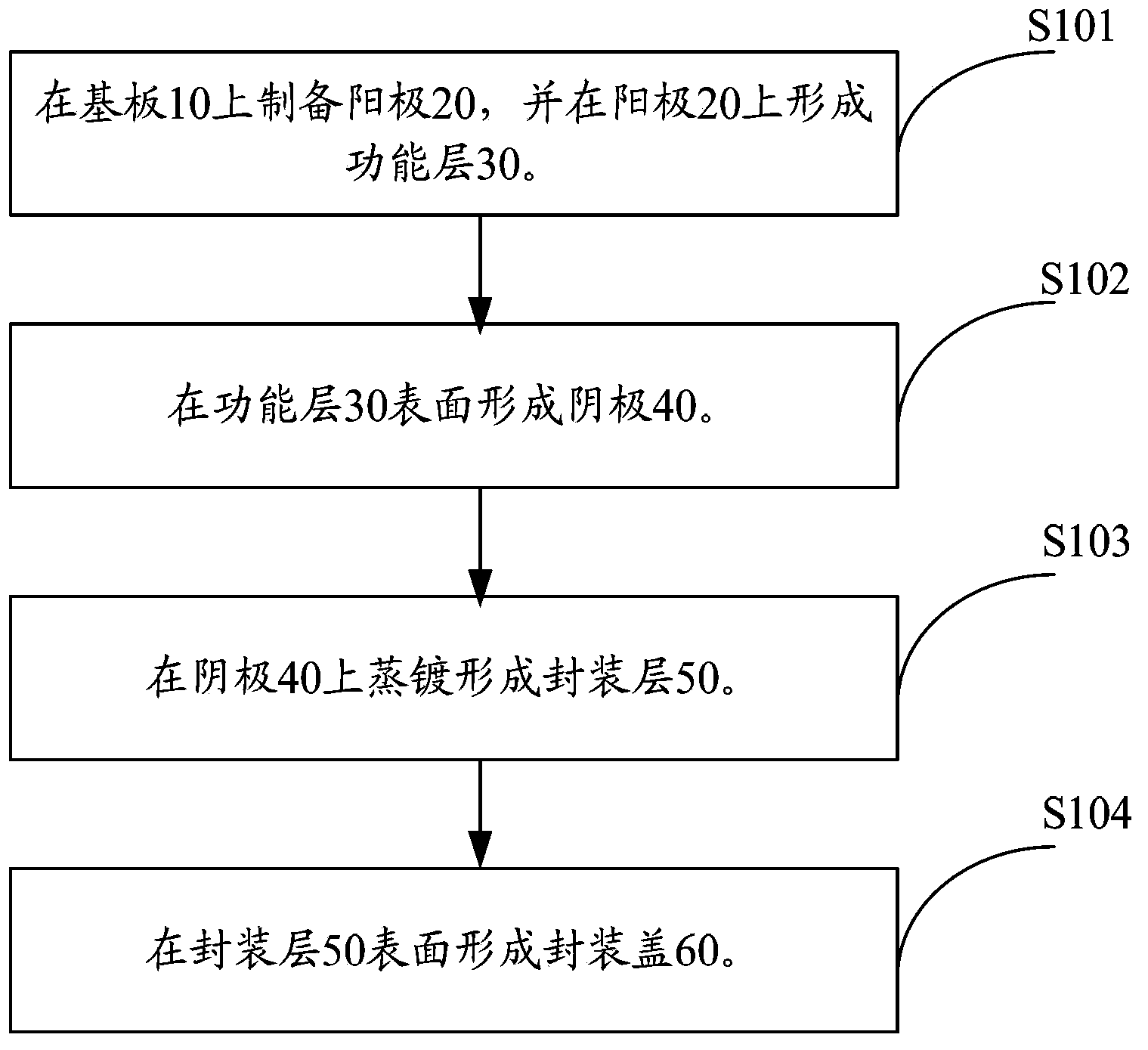
[0059] according to figure 2 It can be known that the preparation method of the organic electroluminescent device 100 provided by the present invention, the specific steps include:
[0060] S101 prepare an anode 20 on the substrate 10 and form a functional layer 30 on the anode 20 .
[0061] The functional layer 30 includes a hole injection layer, a hole transport layer, a light emitting layer, an electron transport layer, and an electron injection layer stacked in sequence.
[0062] The substrate 10 may be a glass substrate or an organic polyethylene terephthalate (PET) film substrate. The substrate 10 has an anode 20 prepared therein, and the anode 20 is an ITO layer. The thickness of the ITO layer is 100nm~150nm.
[0063] Before forming the anode 20 and the functional layer 30 , the surface of the substrate 10 is pretreated to remove pollutants on the surface of the substrate 10 , and the surface is activated to increase the oxygen content on the surface of the substrat...
Embodiment 1
[0086] A method for preparing an organic electroluminescent device, comprising the following steps:
[0087] 1. Substrate pretreatment and anode preparation: Use acetone, ethanol, deionized water and ethanol in sequence to clean with an ultrasonic cleaner. The cleaning time for each washing is 5 minutes, then blow dry with nitrogen, and use an oven to dry before use ; ITO glass is arranged on the substrate, and the substrate loaded with ITO glass is subjected to surface activation treatment to increase the oxygen content of the surface layer and improve the work function of the anode surface; the thickness of the ITO glass is 100nm;
[0088] 2. Preparation of functional layer:
[0089] Evaporating a hole injection layer on the anode;
[0090] The material of the hole injection layer includes N,N'-di(1-naphthyl)-N,N'-diphenyl-1,1'-biphenyl-4-4'-diamine (NPB) and doped Molybdenum oxide (MoO 3 ). MoO 3 The mass percentage content is 30%. The thickness of the hole injection ...
Embodiment 2
[0113] A method for preparing an organic electroluminescent device, comprising the following steps:
[0114] 1,2,3 are the same as embodiment 1;
[0115] 4. Preparation of encapsulation layer:
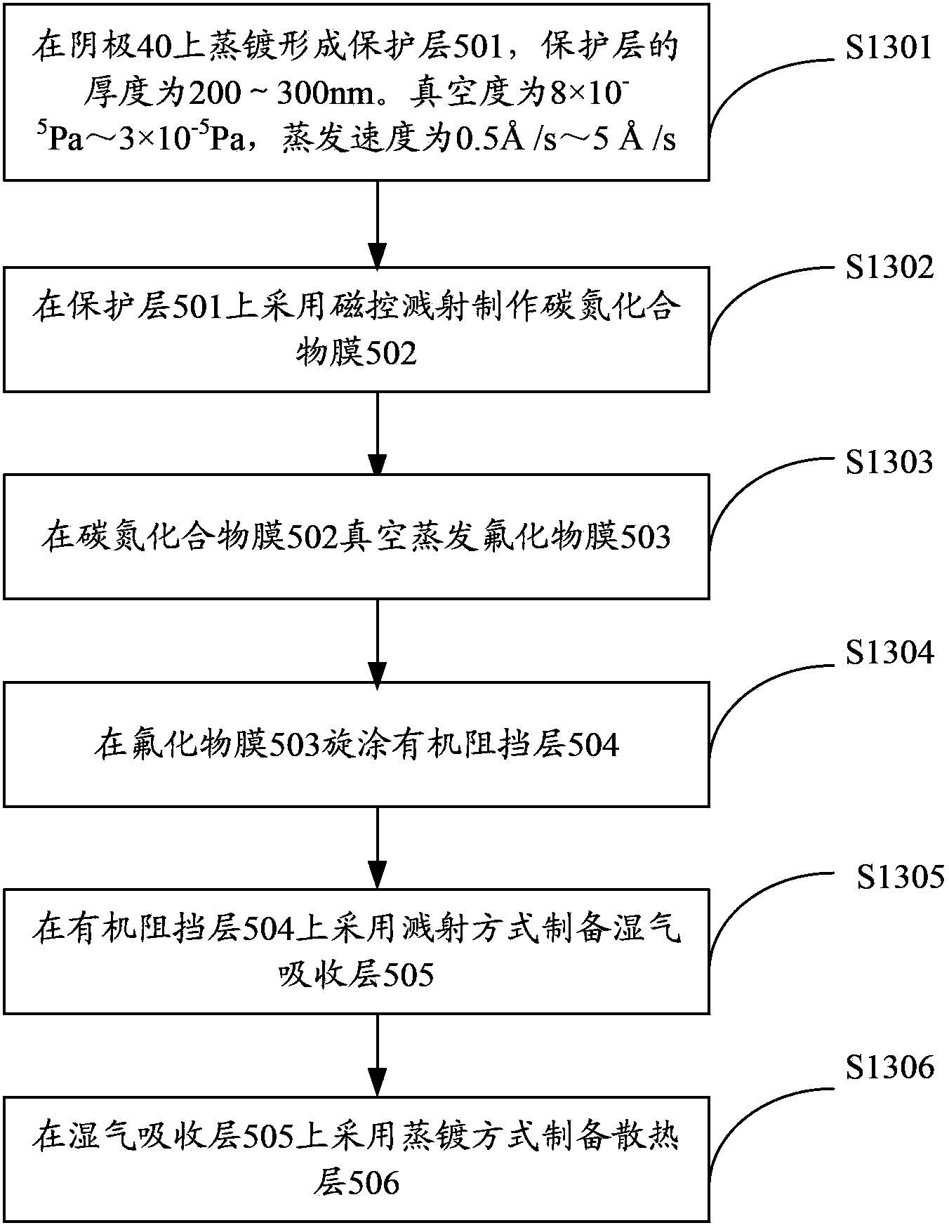
[0116] An encapsulation layer is provided on the cathode, and the encapsulation layer includes a protective layer, a carbonitride film, an organic barrier layer, a moisture absorption layer and a heat dissipation layer;
[0117] Evaporate on the cathode to form a protective layer. The material of the protective layer is N, N'-(1-naphthyl)-N, N'-diphenyl-4,4'-biphenylenediamine, and the thickness of the protective layer is 300nm. Evaporation condition is, vacuum degree is 3×10 -5 Pa, the evaporation rate is
[0118] Magnetron sputtering is used to make a carbonitride film on the protective layer. The carbonitride film is a nitride film doped with carbide, wherein the carbide material is tungsten carbide, and the nitride material is aluminum nitride. The carbide and The mass ratio...
PUM
| Property | Measurement | Unit |
|---|---|---|
| Thickness | aaaaa | aaaaa |
| Thickness | aaaaa | aaaaa |
| Thickness | aaaaa | aaaaa |
Abstract
Description
Claims
Application Information
 - R&D
- Intellectual Property
- Life Sciences
- Materials
- Tech Scout
- Unparalleled Data Quality
- Higher Quality Content
- 60% Fewer Hallucinations
Browse by: Latest US Patents, China's latest patents, Technical Efficacy Thesaurus, Application Domain, Technology Topic, Popular Technical Reports.
© 2025 PatSnap. All rights reserved.Legal|Privacy policy|Modern Slavery Act Transparency Statement|Sitemap|About US| Contact US: help@patsnap.com


