Graphene thin film touch sensor and manufacturing method thereof
A technology of graphene film and touch sensor, which is applied in the direction of instruments, electrical digital data processing, and input/output process of data processing, etc. It can solve the problems of insufficient adhesion and difficulty in meeting the processing requirements of touch screens, etc.
- Summary
- Abstract
- Description
- Claims
- Application Information
AI Technical Summary
Problems solved by technology
Method used
Image
Examples
Embodiment 1
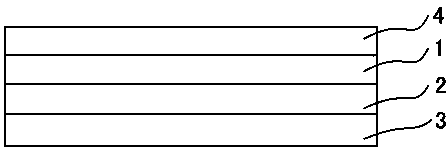
[0028] like figure 1 As shown, a graphene film touch sensor described in the embodiment of the present invention mainly includes a substrate 3, a metal lead electrode 2 and a graphene film 1, and also includes an optically transparent glue 4, and the metal lead electrode 2 is arranged on the surface of the substrate. The graphene film 1 is directly covered on the metal lead electrode 2 , and the optically transparent adhesive 4 is attached to the surface of the graphene film 1 .
[0029] A preferred embodiment, the material of the base 3 is polyethylene phthalate, polycarbonate, polyvinyl chloride, polyethylene, polyethylene naphthalate, polymethyl methacrylate, quartz or Any one of glass is acceptable.
[0030] The material of the metal lead electrode 2 is at least one of copper, silver, cobalt, gold, nickel, chromium, zinc, iron, platinum, ruthenium, molybdenum, niobium, iridium, palladium, titanium, pickaxe, tungsten, vanadium, aluminum, bismuth It can be any one of the a...
Embodiment 2
[0044] The embodiment of the present embodiment is basically the same as that of Example 1, except that the graphene film 1 is 100 layers, the thickness of the graphene film 1 is 30nm, and the optical transmittance in the visible light segment is 0%; The surface of the ethylene glycol ester substrate is sputtered with metal, using the vacuum evaporation method, followed by a three-layer metal stack of copper, aluminum and copper, the metal thickness is 10nm, 200nm, 50nm, and the square resistance of the metal lead electrode is 0.35Ω / □.
Embodiment 3
[0046] The embodiment of this embodiment is basically the same as that of Example 1, the difference is that the graphene film 1 is 2 layers, the thickness of the graphene film 1 is 0.7nm, and the optical transmittance in the visible light segment is 95%; The metal is sputtered on the surface of the ethylene glycol formate substrate, using the vacuum magnetron sputtering method, followed by a three-layer metal stack of copper, nickel and copper, the metal thickness is 20nm, 200nm, 40nm, and the square resistance of the metal lead electrode is 0.3Ω / □.
PUM
| Property | Measurement | Unit |
|---|---|---|
| thickness | aaaaa | aaaaa |
| thickness | aaaaa | aaaaa |
| thickness | aaaaa | aaaaa |
Abstract
Description
Claims
Application Information
