Method for manufacturing PERT crystalline silicon solar battery by adopting novel doping mode

A technology of solar cells and manufacturing methods, applied in circuits, photovoltaic power generation, electrical components, etc., can solve problems such as undetermined process methods, and achieve the effects of reducing equipment investment, saving costs, and being easy to operate

Inactive Publication Date: 2014-08-20
ALTUSVIA ENERGY TAICANG
View PDF4 Cites 16 Cited by
  • Summary
  • Abstract
  • Description
  • Claims
  • Application Information

AI Technical Summary

Problems solved by technology

[0007] Although the battery structure was proposed by the University of New South Wales in Australia as early as the 1990s, a process method suitable for industrial production has not been determined.

Method used


Image

  • Method for manufacturing PERT crystalline silicon solar battery by adopting novel doping mode

Examples


Embodiment 1

[0041] A method for manufacturing a PERT crystalline silicon solar cell using a novel doping method, comprising the following steps:

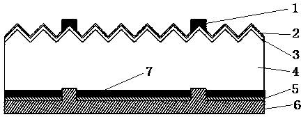
[0042] (1) Single-sided texturing of silicon wafers, cleaning: select P-type silicon wafers, use 156mm P-type single crystal silicon wafers as the base material, and use 0.6% sodium hydroxide or Potassium hydroxide solution is chemically etched at 76°C to prepare a pyramid-shaped suede surface, which is then cleaned with 5% hydrofluoric acid to remove surface impurities;

[0043] (2) Deposit phosphosilicate glass on the front side: Deposit phosphosilicate glass (PSD) on the front side of the silicon wafer by atmospheric pressure chemical vapor deposition (APCVD), and print phosphorous paste by screen printing with a spraying mass fraction of 5% phosphoric acid aqueous solution, and finally deposit a 50nm phosphosilicate glass layer on the front side of the silicon wafer;

[0044] (3) Depositing borosilicate glass on the back side: Borosilicate...

Embodiment 2

[0055]A method for manufacturing a PERT crystalline silicon solar cell using a novel doping method, comprising the following steps:

[0056] (1) Single-sided texturing of silicon wafers, cleaning: select P-type silicon wafers, use 156mm P-type single crystal silicon wafers as the base material, and use 1% sodium hydroxide or Potassium hydroxide solution is chemically etched at 80°C to prepare a pyramid-shaped suede surface, which is then cleaned with hydrofluoric acid with a mass fraction of 10% to remove surface impurities;

[0057] (2) Depositing phosphosilicate glass on the front side: Depositing phosphosilicate glass (PSD) on the front side of the silicon wafer by atmospheric pressure chemical vapor deposition (APCVD), printing phosphorous paste by screen printing, and spraying a mass fraction of 10% phosphoric acid aqueous solution, and finally deposit a 200nm phosphosilicate glass layer on the front side of the silicon wafer;

[0058] (3) Depositing borosilicate glass o...

Embodiment 3

[0069] A method for manufacturing a PERT crystalline silicon solar cell using a novel doping method, comprising the following steps:

[0070] (1) Single-sided texturing of silicon wafers, cleaning: select P-type silicon wafers, use 156mm P-type single crystal silicon wafers as the base material, and use 1.8% sodium hydroxide or Potassium hydroxide solution is chemically etched at 85°C to prepare a pyramid-shaped suede surface, which is then cleaned with 25% hydrofluoric acid to remove surface impurities;

[0071] (2) Deposit phosphosilicate glass on the front side: Deposit phosphosilicate glass (PSD) on the front side of the silicon wafer by atmospheric pressure chemical vapor deposition (APCVD), and print phosphorous paste by screen printing, with a spraying mass fraction of 45% phosphoric acid aqueous solution, and finally deposit a 450nm phosphosilicate glass layer on the front side of the silicon wafer;

[0072] (3) Deposit borosilicate glass on the back side: Borosilicat...


PUM

PropertyMeasurementUnit
thicknessaaaaaaaaaa
thicknessaaaaaaaaaa
thicknessaaaaaaaaaa

Abstract

The invention provides a method for manufacturing a PERT crystalline silicon solar battery by adopting a novel doping mode. The method comprises the steps that texturing is carried out on the single face of a silicon chip, cleaning is carried out, phosphorosilicate glass deposits on the front, borosilicate glass deposits on the back, high-temperature annealing is carried out, n doping layers are formed on the front, p doping layers are formed on the back, plasma edge etching is carried out, the phosphorosilicate glass and the borosilicate glass remaining on the surface of the silicon chip are cleaned and removed, an aluminum oxide/silicon nitride laminating film deposits on the single face of the back, a silicon nitride antireflection film deposits on the front, the film is partially opened from the back so that the boron doping layers can be exposed, a back electrode and an aluminum layer are printed on the back, a silver grid line is printed on the front, and sintering and testing are carried out. The preparing method is simple in step, easy to operate, and capable of efficiently manufacturing the crystalline silicon solar battery in a mass mode, and has the advantages that on the basis of commercialized industrial equipment, conventional battery production equipment possessed by an enterprise production line at present is fully utilized, the equipment investment is greatly reduced, and the manufacturing cost of per watt of the battery is not increased.

Description

technical field [0001] The invention belongs to the field of crystalline silicon solar cell manufacturing, and relates to a method for manufacturing a high-efficiency crystalline silicon solar cell with full-surface doping on the back and back passivation and back point contact, in particular to a PERT crystalline silicon adopting a new doping method How to make solar cells. Background technique [0002] Against the backdrop of increasingly prominent problems such as energy scarcity, resource shortage, and environmental pollution, the use of natural resources for solar power generation has been regarded as a countermeasure to solve the problems of global warming and fossil fuel depletion, and has been favored by countries all over the world. However, the high production cost restricts its application range, and with the sharp reduction of government subsidies, reducing the production cost of cells and improving power generation efficiency has become an urgent issue for manuf...

Claims


Application Information

Patent Timeline
Patent Type & Authority Applications(China)
IPC IPC(8): H01L31/18
CPCH01L31/1804Y02E10/547Y02P70/50
Inventor 夏正月高艳涛崔会英钱亮何锐陈同银刘仁中董经兵张雪谢烜张斌邢国强
Owner ALTUSVIA ENERGY TAICANG
Why Eureka
Try Eureka