Organic ultraviolet light detector taking HATCN and Cu (I) complex prepared by HATCN as anode buffer layer

A technology of anode buffer layer and organic ultraviolet light, which is applied in the direction of electric solid device, semiconductor device, semiconductor/solid device manufacturing, etc., to achieve the effect of facilitating hole transport, preventing device aging, and high electron mobility

Inactive Publication Date: 2014-09-17
JILIN NORMAL UNIV
View PDF3 Cites 2 Cited by
  • Summary
  • Abstract
  • Description
  • Claims
  • Application Information

AI Technical Summary

Problems solved by technology

[0004] In order to solve the device aging of the organic ultraviolet light detection device in the above-mentioned background technology, improve the stability of the device, the working life and the detection performance, etc., the purpose of the present invention is to combine a class of HATCN with higher electron mobility and low LUMO energy level The Cu(I) complex constructed by it is used in organic ultraviolet photodetection devices to improve device performance and life, etc., and the synthesis method of the copper complex is simple, and the device is easy to prepare

Method used


Image

  • Organic ultraviolet light detector taking HATCN and Cu (I) complex prepared by HATCN as anode buffer layer
  • Organic ultraviolet light detector taking HATCN and Cu (I) complex prepared by HATCN as anode buffer layer
  • Organic ultraviolet light detector taking HATCN and Cu (I) complex prepared by HATCN as anode buffer layer

Examples


preparation example Construction

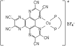
[0052] ②. Preparation of Cu(I) complex Ⅰ (preparation of Cu(I) complex CuDH):

[0053] With 538.6mg (1.0mmol) two (2-diphenylphosphino) phenyl ether, 314.0mg (1.0mmol) [Cu (CH 3 EN) 4 ] BF 4 Dissolve in 10ml of dichloromethane, stir at room temperature for about 30 minutes, then add 384.3mg (1.0mmol) HATCN, and continue stirring for one hour. The final solution was rotary evaporated, and the obtained solid powder was CuDH.

[0054] ③. Preparation of Cu(I) complex II (preparation of Cu(I) complex CuBH):

[0055] With 446.5mg (1.0mmol) 1,2-bis (diphenylphosphino) benzene, 314.0mg (1.0mmol) [Cu (CH 3 EN) 4 ] BF 4 Dissolve in 10ml of dichloromethane, stir at room temperature for about 30 minutes, then add 384.3mg (1.0mmol) HATCN, and continue stirring for one hour. The final solution was rotary evaporated, and the obtained solid powder was CuBH.

Embodiment 1

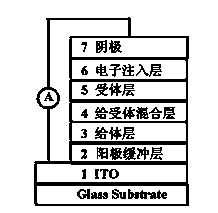
[0057] select figure 1 The device structure shown, in the present embodiment, first on the ITO anode 1, the anode buffer layer HATCN with a thickness of 7nm is vacuum-deposited, then on the anode buffer layer 2, an electron donor layer 3 of 30nm is deposited, and then on the electron donor A mixed layer 4 of electron donor and electron acceptor with a weight ratio of 1:1 and a thickness of 40 nm is deposited on layer 3, and then a 40 nm electron acceptor layer 5 is deposited on the mixed layer 4, followed by a 1 nm electron injection layer 6 , and finally deposited a 200nm metallic Al cathode. All the above films are deposited by vacuum coating process, the thickness of the film is monitored by a film thickness monitor, and the external circuit is detected by KEITHLEY2601.

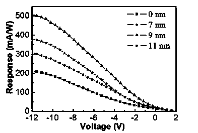
[0058] Effect: at a light intensity of 1.05mW / cm 2 , Under the irradiation of ultraviolet light with a center wavelength of 365nm and an external reverse bias of -12V, the photocurrent response value of ...

Embodiment 2

[0060] On the basis of Example 1, the thickness of the anode buffer layer 2 was changed to 9 nm, and other manufacturing conditions remained unchanged.

[0061] Effect: at light intensity 1.05mW / cm 2 , Under the irradiation of light with a central wavelength of 365nm and an external reverse bias of -12V, the photocurrent response value of the device is 508mA / W (see figure 2 ), the current density is 0.53mA / cm 2 .


PUM


Abstract

The invention belongs to the organic photoelectric material and organic ultraviolet light detector field and relates to an organic ultraviolet light detector taking HATCN and a Cu (I) complex prepared by the HATCN as an anode buffer layer. A structure of the detector sequentially comprises an ITO anode, an anode buffer layer, an electron donor layer, a mixed donor and acceptor layer, an electron acceptor layer, an electron injecting layer and a cathode. The detector is characterized in that the HATCN and the Cu (I) complex prepared by the HATCN have relatively high electron mobility and relatively good film forming ability and stability, electrons are facilitated through quite low LUMO energy level to shuttle among HOMO energy levels of the anode and the donor, so the electrons and excitons can realize rapid dissociation to form cavity composition, cavity transmission is further facilitated by charge composition mechanism, and thereby performance of the detector is improved. According to the detector, by employing the material of the anode buffer layer, performance of the organic ultraviolet light detector is greatly improved, aging of the organic ultraviolet light detector is slowed down, and stability of the organic ultraviolet light detector is improved.

Description

technical field [0001] The invention belongs to the field of materials and devices for organic ultraviolet photodetection devices, and specifically relates to a class of HATCN with high electron transport performance and Cu(I) complexes (monovalent copper complexes) constructed therefrom as anode buffer layer materials Organic UV photodetectors. Background technique [0002] Ultraviolet light detection device is a device that converts ultraviolet light into electrical signals, and has important applications in various fields such as military affairs, medical treatment, and the environment. Before the 1980s, the research on ultraviolet light detection devices mainly focused on inorganic semiconductors with wide band gaps such as GaN and SiC. The fabrication process of such ultraviolet light detection devices was complicated and costly. In recent years, ultraviolet light detection devices based on organic semiconductors have attracted widespread attention due to their wide se...

Claims


Application Information

Patent Timeline
Patent Type & Authority Applications(China)
IPC IPC(8): H01L51/46H01L51/42
CPCY02E10/549H10K85/371H10K30/20
Inventor 车广波刘敏刘春波苏斌徐占林孔治国
Owner JILIN NORMAL UNIV
Why Eureka
Try Eureka