Packaging lead wire material structure and processing method thereof

A wire material and processing method technology, applied in semiconductor devices, semiconductor/solid-state device manufacturing, semiconductor/solid-state device components, etc., can solve the problems of poor yield, slow speed, complex circuits, etc., and improve the ability of electron transmission , Reduce the amount of gold used, the effect of low thermal expansion coefficient

Active Publication Date: 2014-11-05
SUNPHIRE OPT TRONIC
View PDF6 Cites 0 Cited by
  • Summary
  • Abstract
  • Description
  • Claims
  • Application Information

AI Technical Summary

Problems solved by technology

However, due to the fact that the hardness of copper is higher than that of gold, when copper wire bonding is used in IC packaging, due to the complex circuit, fragile structure, and thin and dense pins, the difficulty of wire bonding technology is greatly increased, and the investment in R & D and certification is not easy to recover.
[0004] As we all know, copper wire is very easy to oxidize, and special attention must be paid to the isolation of air during storage and transportation, and extremely strict inert gas protection is required during the wire bonding process; what is more serious is that due to the easy oxidation and corrosion characteristics of copper wire, It will lead to low reliability of wire bonding products. On the other hand, because of the high strength and hardness of copper wire, its welding operation parameters are narrow, the speed is slow and the yield rate is poor, especially in the recent very popular In the ball bonding package, the copper wire encounters great difficulties, forcing the packaging factory to adopt the workaround of "gold and copper mixing", but it still cannot completely overcome the poor quality of the ball stacking at the gold / copper interface

Method used


Image

  • Packaging lead wire material structure and processing method thereof
  • Packaging lead wire material structure and processing method thereof

Examples


Embodiment Construction

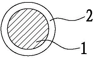
[0020] Such as figure 1 As shown, the structure of a package wire material disclosed by the present invention is composed of an intermediate core 1 and a surface coating 2, the intermediate core 1 is a tungsten wire, the diameter of the tungsten wire is preferably 12.7 microns, the surface coating 2 is gold, and the surface coating The thickness is preferably 2 microns, thereby forming a structure of tungsten inside and gold outside.

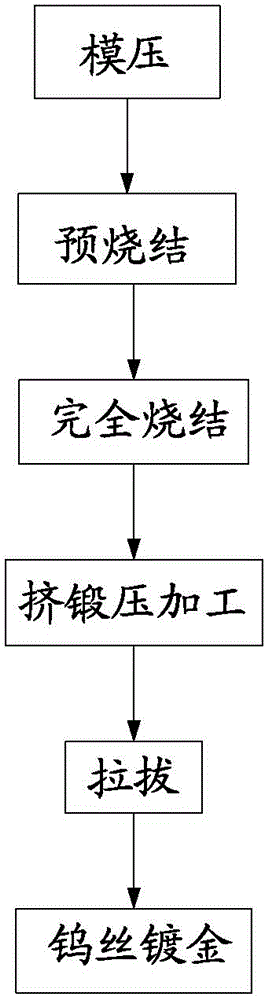
[0021] Such as figure 2 As shown, a packaging wire material disclosed in the present invention is processed according to the following steps.

[0022] The first step, molding.

[0023] Put a fixed weight of tungsten powder into a stainless steel mold and extrude it into a whole rod.

[0024] The second step is pre-sintering.

[0025] Place the fragile rod in the first step in a refractory metal vessel and put it into a hydrogen sintering furnace at a high temperature of 1200-1600°C to continuously agglomerate the metal particles; during thi...


PUM

PropertyMeasurementUnit
Diameteraaaaaaaaaa
Thicknessaaaaaaaaaa
Diameteraaaaaaaaaa

Abstract

The invention discloses a packaging lead wire material structure which consists of a middle wire core and a surface coating, wherein the middle wire core is a tungsten filament, and the surface coating is gold. A processing method comprises the steps of performing die pressing: extruding tungsten powder into a whole bar, performing presintering: placing the bar in a hydrogen sintering furnace, allowing metal particles to be agglomerated at a high temperature and allowing the compactness to reach about 60-70%, performing complete sintering in a vertical sintering furnace, allowing the compactness of the tungsten bar to reach about 85-95%, forming tungsten crystal in the bar, performing power cutoff and cooling, performing extruding, forging and pressing processing, hammering the bar with a hammering machine until the diameter reaches 6350-2540 micrometers, drawing the bar by a wire drawing die to allow the diameter of the bar to reach 12.7 micrometers, preparing the tungsten filament, plating gold on the tungsten filament: allowing the gold plating thickness to be about 2 micrometers, and preparing the packaging lead wire material structure with an internal tungsten and external gold structure. According to the packaging lead wire material structure, a problem derived by using copper is avoided, the consumption of gold is reduced, and the cost is lowered.

Description

technical field [0001] The invention relates to semiconductor and LED rear-end packaging technology, in particular to a structure of packaging wire material and a processing method thereof. Background technique [0002] The internal bonding methods of integrated circuit (Integrated Circuit; IC) packages can be divided into wire bonding, tape-and-reel automatic bonding and flip-chip bonding. Among them, wire bonding is currently the most widely used due to its mature manufacturing process, low cost, and high wiring flexibility. Wide range of bonding technology, accounting for about 90% of all packaged products. [0003] The wires used in wire bonding are divided into gold wires, copper wires and aluminum wires. At present, gold wires are the mainstream because gold has the advantages of high stability, soft quality, and good ductility. It is used for IC packaging wire bonding. When bonding, its yield rate, production efficiency, and wire diameter miniaturization are all quit...

Claims


Application Information

Patent Timeline
IPC IPC(8): H01L23/49H01L21/60
CPCH01L24/45H01L2224/45184H01L2224/45565H01L2224/45644H01L2224/45H01L2224/45015H01L2924/20751H01L2924/00014H01L2924/00012
Inventor 刘伯彦周斌钟其龙王晓靁刘崇志
Owner SUNPHIRE OPT TRONIC
Why Eureka
Try Eureka