Method for manufacturing size-controllable two-dimensional nanostructure of CrN nanopore array

A technology of two-dimensional nanostructure and nanohole array, which is applied in the direction of nanotechnology, nanotechnology, nanotechnology for materials and surface science, etc., can solve the problem of low anti-adhesive effect, achieve no pollution, simple equipment, surface smooth effect

Inactive Publication Date: 2014-11-12
NINGBO UNIVERSITY OF TECHNOLOGY
View PDF1 Cites 2 Cited by
  • Summary
  • Abstract
  • Description
  • Claims
  • Application Information

AI Technical Summary

Problems solved by technology

[0006] However, there are still many deficiencies in the current prior art, including the anti-stick effect (high contact angle and low surface free energy) of nano-mold preparation to be solved. Therefore, the development of new low surface free energy coating materials has been Be the key to improved performance

Method used


Image

  • Method for manufacturing size-controllable two-dimensional nanostructure of CrN nanopore array
  • Method for manufacturing size-controllable two-dimensional nanostructure of CrN nanopore array
  • Method for manufacturing size-controllable two-dimensional nanostructure of CrN nanopore array

Examples


Embodiment 1

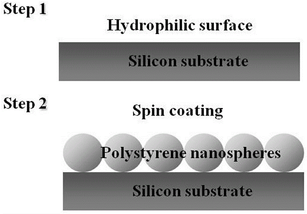
[0031] Embodiment 1 includes the following steps: (1) immersing the silicon substrate into a volume ratio of 1:1 ammonia water (NH 4 OH) and hydrogen peroxide (H 2 o 2 ) in the mixed solution, perform ultrasonic cleaning for 30 minutes, and then wash with deionized water for 10 minutes.

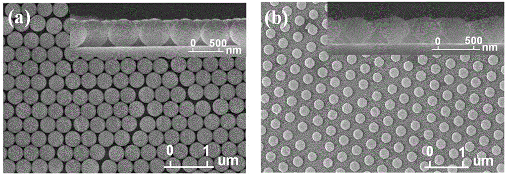
[0032] (2) Using polystyrene (PS) as the polymer raw material, use a spin coater for spin coating, set the speed at 1200 rpm, and proceed for 4 min. After stopping, you can get a self-assembled periodically arranged polystyrene Ethylene (PS) nanosphere monolayer template such as image 3 (a) shown.

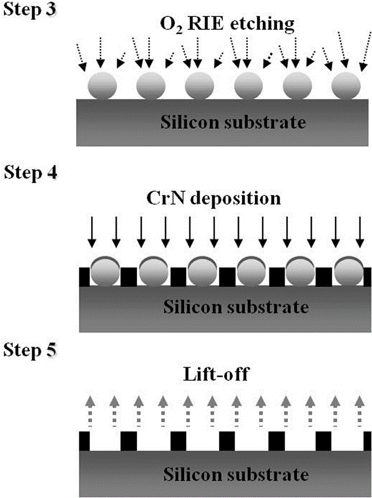
[0033] (3) The size of the nanospheres on the single-layer template was adjusted by reactive ion etching. The power parameters were set to 50W, the etching time was 10min, and oxygen was used as the etching gas to obtain the size-controlled polystyrene nanospheres. layer template.

[0034] (4) Then use the closed-field unbalanced magnetron sputtering ion plating system (CBUBMIP) to install t...

Embodiment 2

[0037] Embodiment 2 includes the following steps: (1) immersing the silicon substrate into a volume ratio of 1:1 ammonia water (NH 4 OH) and hydrogen peroxide (H 2 o 2 ) in the mixed solution, perform ultrasonic cleaning for 30 minutes, and then wash with deionized water for 10 minutes.

[0038] (2) Using polystyrene (PS) as the polymer raw material, use a spin coater for spin coating, set the speed at 1200 rpm, and proceed for 4 min. After stopping, you can get a self-assembled periodically arranged polystyrene Ethylene (PS) nanosphere monolayer template such as image 3 (a) shown.

[0039] (3) The size of the nanospheres on the single-layer template is controlled by reactive ion etching, the power parameter is set to 50W, the etching time is 20min, and oxygen is used as the etching gas, such as image 3 (b) shows the polystyrene nanosphere monolayer template after size regulation.

[0040] (4) Then use the closed-field unbalanced magnetron sputtering ion plating system...

Embodiment 3

[0044] Embodiment 3 includes the following steps: (1) immersing the silicon substrate in a volume ratio of 1:1 ammonia water (NH 4 OH) and hydrogen peroxide (H 2 o 2 ) in the mixed solution, perform ultrasonic cleaning for 30 minutes, and then wash with deionized water for 10 minutes.

[0045] (2) Using polystyrene (PS) as the polymer raw material, use a spin coater for spin coating, set the speed at 1200 rpm, and proceed for 4 min. After stopping, you can get a self-assembled periodically arranged polystyrene Ethylene (PS) nanosphere monolayer template such as image 3 (a) shown.

[0046] (3) The size of the nanospheres on the single-layer template was adjusted by reactive ion etching. The power parameter was set to 50W, the etching time was 25min, and oxygen was used as the etching gas to obtain a single layer of polystyrene nanospheres after size adjustment. template.

[0047] (4) Then use the closed-field unbalanced magnetron sputtering ion plating system (CBUBMIP) to...


PUM

PropertyMeasurementUnit
diameteraaaaaaaaaa
diameteraaaaaaaaaa
diameteraaaaaaaaaa

Abstract

The invention discloses a method for manufacturing a size-controllable two-dimensional nanostructure of a CrN nanopore array. The method for manufacturing the size-controllable two-dimensional nanostructure of the CrN nanopore array comprises the following steps that (1) a substrate is placed in a mixed solution of ammonia water and hydrogen peroxide, and then hydrophilia treatment is conducted by means of ultrasonic waves; (2) a single-layer template on which macromolecular nanoballs are arranged periodically is manufactured on the substrate according to a rotary coating method; (3) the macromolecular nanoballs are etched with oxygen as the etching treatment gas, and then a new single-layer template is obtained after etching; (4) CrN sputtering deposition are conducted on the single-layer template obtained after etching in the step (3) through a closed field non-equilibrium magnetron sputtering ion plating system; (5) the template obtained after deposition in the step (4) is placed in organic solvent, and then the macromolecular nanoballs are dissolved away. According to the method for manufacturing the size-controllable two-dimensional nanostructure of the CrN nanopore array, an array template is manufactured by combining the nanoball rotary-coating technology and the nanoball photoetching method, and the array temperature with the size precision accurately controllable can be manufactured by adjusting the technological conditions.

Description

technical field [0001] The invention belongs to the technical field of material preparation, and in particular relates to a method for controlling the size of a two-dimensional nanostructure of a CrN nanohole array. Background technique [0002] In recent years, research on periodic nanostructure arrays has received more and more attention. Several techniques capable of fabricating periodic nanostructure arrays include electrochemical etching, X-ray etching methods, electron beam etching (EBL) and molecular beam epitaxy. (MBE), etc. Although etching technology can control the morphology of these arrays, its high cost and complicated process limit its application. Therefore, many researchers have tried to develop low-cost, high-throughput, high-resolution etching techniques. [0003] As an alternative method, nanoimprint lithography (NIL) has the advantages of low cost and simple fabrication, can produce large-scale nanostructures, and can replicate different stages of nano...

Claims


Application Information

Patent Timeline
Patent Type & Authority Applications(China)
IPC IPC(8): C23C14/06C23C14/02C23C14/35C23C14/58B82Y40/00B82Y30/00
Inventor 吴泓均鲍明东徐雪波
Owner NINGBO UNIVERSITY OF TECHNOLOGY
Why Eureka
Try Eureka