Nanometer silicon film cathode and manufacturing method thereof
A nano-silicon thin film and a manufacturing method technology are applied in cold cathode manufacturing, discharge tube cold cathode, electrode system manufacturing and other directions, which can solve the problem of poor electron emission stability of porous silicon cathode, unstable mechanical and chemical properties, and unfavorable long-term use. devices, etc., to achieve the effects of good electron emission stability, favorable electron acceleration, and high electron emission density
- Summary
- Abstract
- Description
- Claims
- Application Information
AI Technical Summary
Problems solved by technology
Method used
Image

Examples
Embodiment 1
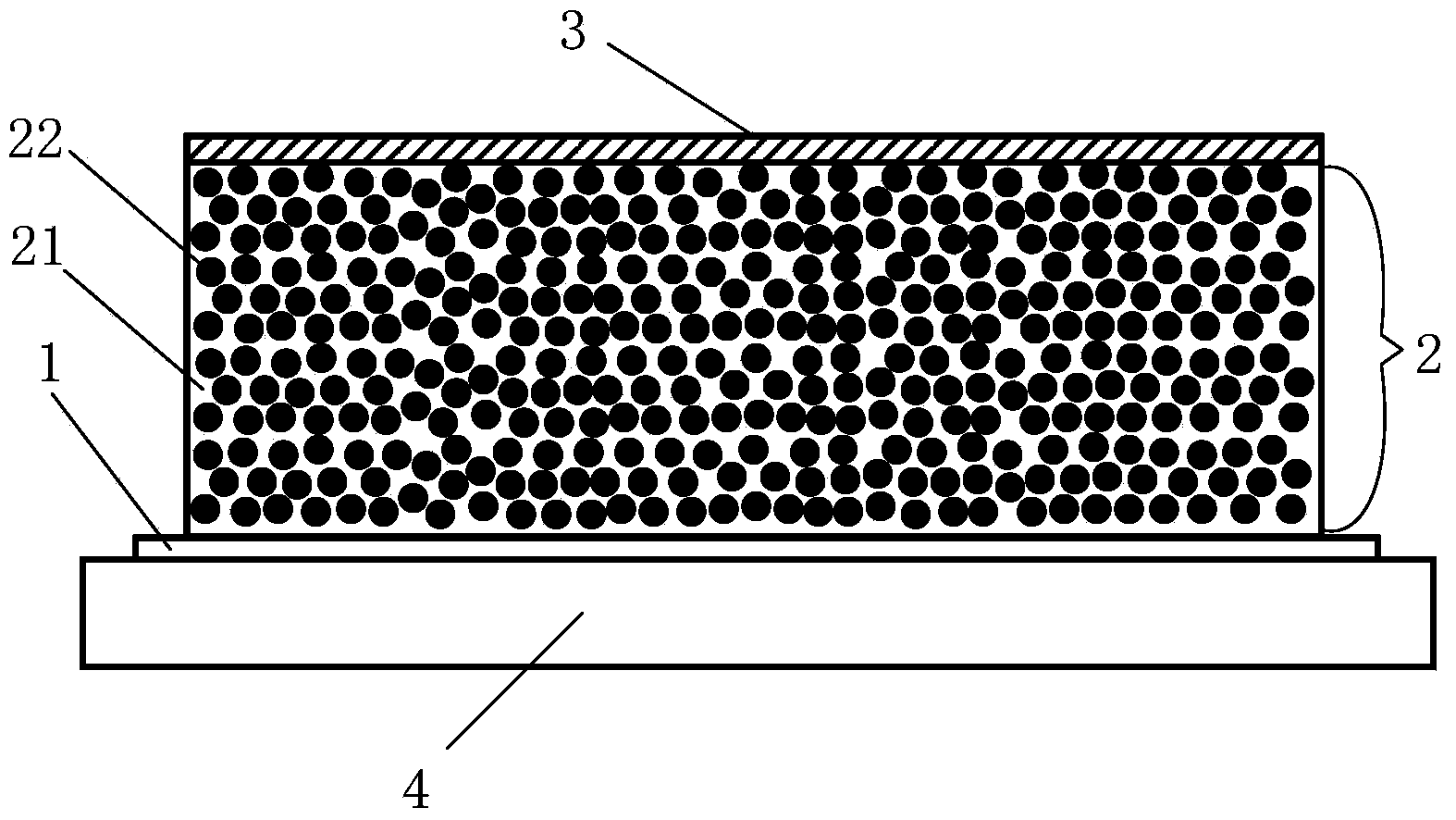
[0065] refer to figure 1 As shown, the nano-silicon thin film cathode has a multi-layer structure, including a bottom electrode 1, a silicon dioxide layer 2 containing nanocrystalline silicon (composed of nanocrystalline silicon 22 and silicon dioxide 21) and a top electrode that are sequentially arranged on a substrate 4 3.
[0066] The fabrication method of the nano-silicon thin film cathode comprises the following steps:
[0067] 1) using a sputtering nickel target to deposit the bottom electrode 1 on the substrate 4, the thickness of which is 200nm;
[0068] 2) Introduce argon and oxygen into the coating chamber so that the partial pressure ratio of argon and oxygen is 5:1 while controlling the total air pressure in the coating chamber to be 0.2Pa, and the temperature of the substrate 4 is controlled at 500°C to The silicon target is used as the sputtering source, and SiO with a thickness of 500 nm is deposited on the bottom electrode 1 with a sputtering power of 160 W. ...
Embodiment 2
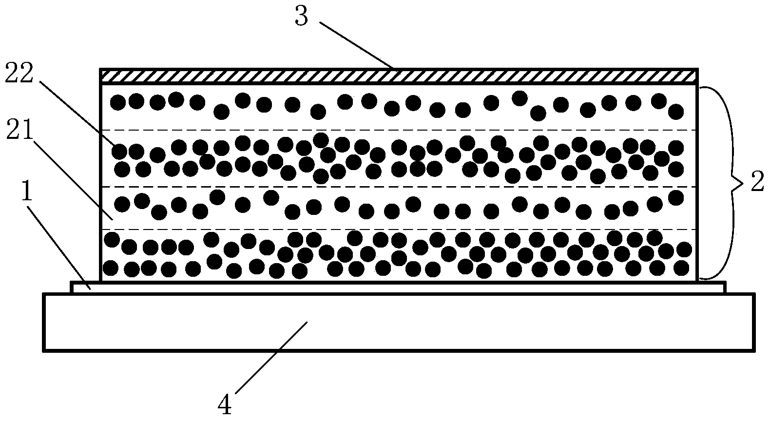
[0071] refer to figure 2 As shown, the nano-silicon thin film cathode has a multi-layer structure, including a bottom electrode 1, a silicon dioxide layer 2 containing nanocrystalline silicon (composed of nanocrystalline silicon 22 and silicon dioxide 21) and a top electrode that are sequentially arranged on a substrate 4 3.
[0072] The fabrication method of the nano-silicon thin film cathode comprises the following steps:
[0073] 1) Depositing the bottom electrode 1 on the substrate 4 with a sputtering aluminum target, the thickness of which is 50 nm;
[0074] 2) Depositing SiO on a silicon target as a sputtering source x During the thin film process, argon and oxygen are introduced into the coating chamber, the total pressure in the coating chamber is controlled at 0.5Pa, and the temperature of the substrate 4 is controlled at 200°C, and the sputtering power of the silicon target is 150W, which is adjusted by time intervals The flow rate of argon and oxygen is such tha...
Embodiment 3
[0077] refer to figure 2 As shown, the nano-silicon thin film cathode has a multi-layer structure, including a bottom electrode 1, a silicon dioxide layer 2 containing nanocrystalline silicon (composed of nanocrystalline silicon 22 and silicon dioxide 21) and a top electrode that are sequentially arranged on a substrate 4 3.
[0078] The fabrication method of the nano-silicon thin film cathode comprises the following steps:
[0079] 1) using a sputtering chromium target to deposit the bottom electrode 1 on the substrate 4, the thickness of which is 300nm;
[0080] 2) Depositing SiO on a silicon target as a sputtering source x During the thin film process, argon and oxygen are introduced into the coating chamber, the total pressure in the coating chamber is controlled at 1.0Pa, the partial pressure ratio of argon and oxygen is 3:1, and the temperature of the substrate 4 is controlled at 350°C. By adjusting the sputtering power of the silicon target in time intervals, the co...
PUM
| Property | Measurement | Unit |
|---|---|---|
| Thickness | aaaaa | aaaaa |
| Thickness | aaaaa | aaaaa |
| Thickness | aaaaa | aaaaa |
Abstract
Description
Claims
Application Information
 - R&D
- Intellectual Property
- Life Sciences
- Materials
- Tech Scout
- Unparalleled Data Quality
- Higher Quality Content
- 60% Fewer Hallucinations
Browse by: Latest US Patents, China's latest patents, Technical Efficacy Thesaurus, Application Domain, Technology Topic, Popular Technical Reports.
© 2025 PatSnap. All rights reserved.Legal|Privacy policy|Modern Slavery Act Transparency Statement|Sitemap|About US| Contact US: help@patsnap.com