

Organic field effect transistor and applications in ultraviolet sensing
A transistor and organic field technology, applied in the field of organic field effect transistors, can solve the problems of inability to judge the wavelength selectivity of materials, low device performance, and no widespread concern, and achieve good device stability and high carrier mobility. , Sensitive effect of detection signal
- Summary
- Abstract
- Description
- Claims
- Application Information
AI Technical Summary
Problems solved by technology
Method used
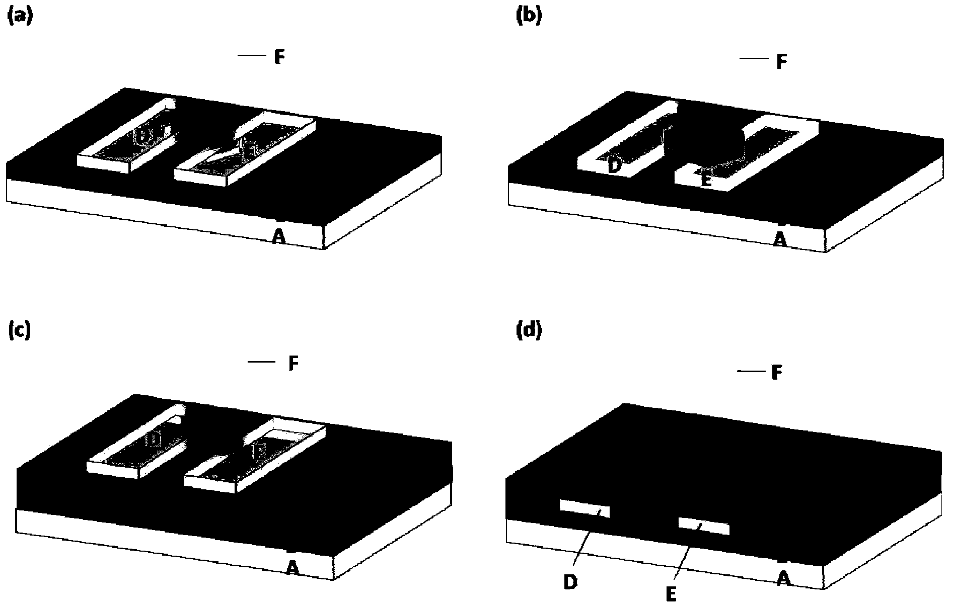
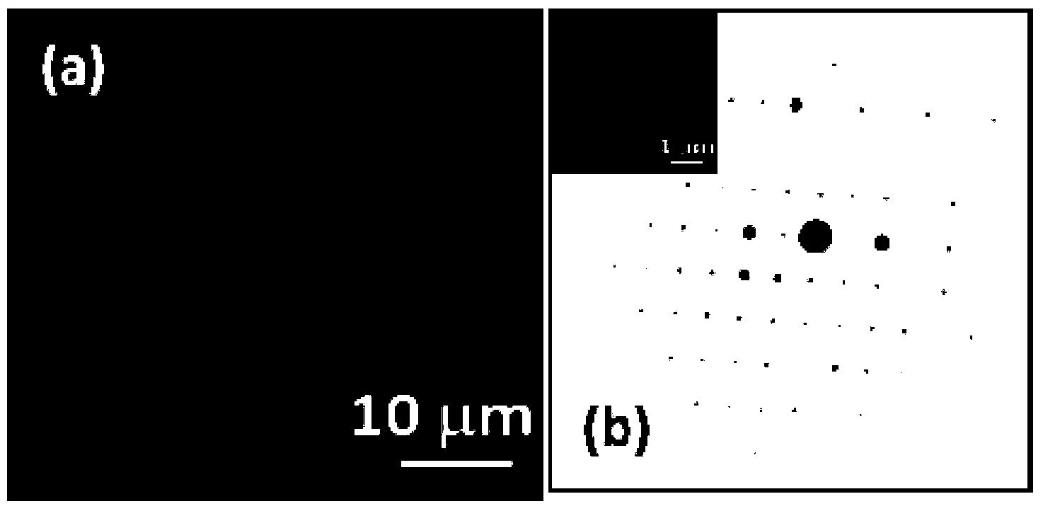
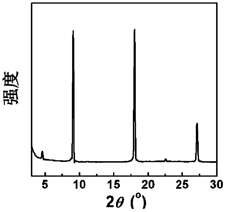
Image

Examples
Embodiment 1
[0082] The preparation of the compound shown in embodiment 1, formula II
[0083] 1) Under nitrogen atmosphere, slowly add n-butyllithium (1.1eq.) into anhydrous solution of benzo[1,2-b:4,5-b']dithiophene (1eq.) cooled to -78℃ In the ether solution, after the temperature of the solution was gradually raised to room temperature and stirred for 3 hours, N,N-dimethylformamide (1.1 eq.) was added and stirred overnight. The reaction solution was quenched with dilute hydrochloric acid aqueous solution, extracted with ether and washed with saturated brine, then fully dried with magnesium sulfate, and the mixture after vacuum spin-drying was separated and purified by column chromatography to obtain benzo[1,2-b:4,5- b'] dithiophene-2-carbaldehyde;
[0084] 2) Slowly add titanium tetrachloride (1.15eq.) to the tetrahydrofuran suspension of zinc powder (2.3eq.) and heat the solution to reflux. After 4 hours, the dissolved benzo[1,2-b:4 ,5-b']dithiophene-2-carbaldehyde (1eq.) and pyridi...
Embodiment 2
[0088] The preparation of the compound shown in embodiment 2, formula III
[0089] a) Under nitrogen atmosphere, slowly add n-butyllithium (1eq.) into benzo[1,2-b:4,5-b']dithiophene (1eq.) in anhydrous THF cooled to -78℃ solution, slowly add I at this temperature 2(1eq.) in tetrahydrofuran, stirred for 12 hours after the mixture rose to room temperature. After the reaction solution was quenched with water, it was filtered and rinsed with a solvent (petroleum ether), and the resulting mixture was separated and purified by column chromatography to obtain 2-iodobenzo[1,2-b:4,5-b']dithiophene;
[0090] b) Add 2-iodobenzo[1,2-b:4,5-b']dithiophene (1eq.), tetrakis(triphenylphosphine)palladium (0.1eq.) and 2,6- Bis(tributyltin)acetylene (0.5 eq.) was slowly added to a solution of di-tert-butyl-4-methylphenol (catalytic amount) in anhydrous toluene, and the reaction solution was heated to reflux and stirred for 1 day. After the reaction solution was cooled to room temperature, the ...
Embodiment 3
[0093] The preparation of the compound shown in embodiment 3, formula IV
[0094] Referring to the method provided in the literature J.Mater.Chem., 2010,20,10931-10935, with 2-iodobenzo[1,2-b:4,5-b']dithiophene and C 12 h 25 MgBr is raw material, prepares and obtains 2-dodecylbenzo[1,2-b:4,5-b'] dithiophene; Then with 2-dodecylbenzo[1,2-b:4, 5-b']dithiophene is used as a raw material to prepare the compound represented by formula IV by referring to the preparation method of the compound represented by formula II above.
[0095]
[0096] The structural characterization data of the compound shown in formula IV: Mp: >300°C; MS (EI) m / z: 740 (M + ); Elemental analysis results: C: 74.31, H: 8.42.
PUM
 Abstract
Description
Claims
Application Information