Preparation method of polymer optical waveguide with inclined-surface coupling port

A technology of coupling ports and polymers, which is applied in the direction of optical waveguide light guides, pattern surface photolithography, and optomechanical equipment, can solve the problems of high cost of background technology, complex processing technology, and small range of change in the length of the gradient area. Achieve the effect of simple and fast process, low cost, and reduce device cost

Inactive Publication Date: 2015-04-08
JILIN UNIV
View PDF5 Cites 8 Cited by
  • Summary
  • Abstract
  • Description
  • Claims
  • Application Information

AI Technical Summary

Problems solved by technology

[0005] The technical problem to be solved by the present invention is to overcome the disadvantages of high cost, complex processing technology and small variation range of the gradient zone length in the background technology, and to find a high-precision, economical, fast and controllable process for preparing polymers with gradient coupling ports. Optical waveguide

Method used


Image

  • Preparation method of polymer optical waveguide with inclined-surface coupling port
  • Preparation method of polymer optical waveguide with inclined-surface coupling port
  • Preparation method of polymer optical waveguide with inclined-surface coupling port

Examples


Embodiment 1

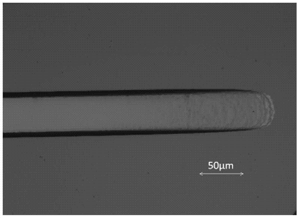
[0045] When the cutting power is 18W, the cutting speed is 10mm / s, the aluminum film thickness is 37nm, the photoresist spin coating revolution is 3000 revolutions, and the gray scale exposure time is 8s, the waveguide embodiment with beveled coupling port

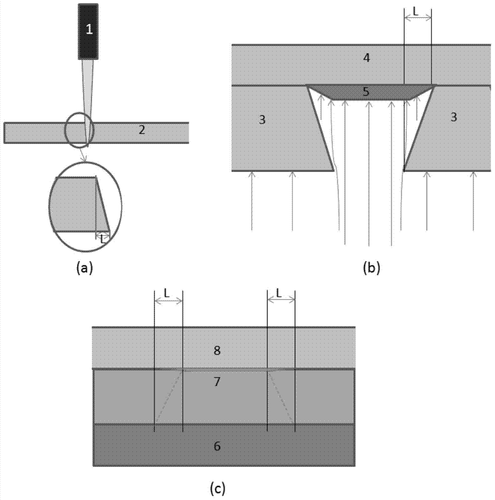
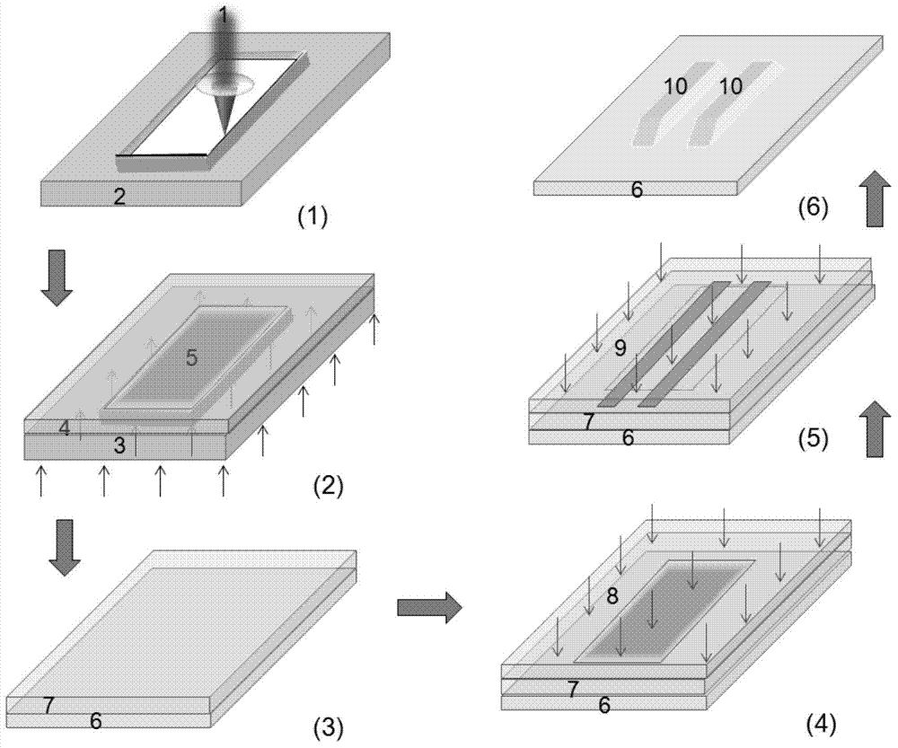
[0046] Mask evaporation mask preparation: select 100.0mm*100.0mm*1.5mm surface-polished methyl methacrylate (PMMA) polymer sheet 2, which is produced by carbon dioxide laser 1 (produced by Shandong Ketai Laser Co., Ltd., maximum power 60W), The cutting speed is 10mm / s, the output power of the carbon dioxide laser is 18W, and the size of the evaporation window is 15mm*10mm (corresponding to the cutting pattern size of the computer corel draw software) to form an evaporation mask 3 with an evaporation window, and then use acetone, ethanol, Wipe the mask with deionized water in turn. The projection length L of the slope on the surface of the sheet is 90 μm.

[0047] A polymer sheet of polymer methyl methacrylate (PMMA) with a siz...

Embodiment 2

[0051] When the cutting power is 21W, the cutting speed is 10mm / s, the aluminum film thickness is 37nm, the photoresist spin coating revolution is 3000 revolutions, and the gray scale exposure time is 8s, the waveguide embodiment with beveled coupling port

[0052] Mask evaporation mask preparation: select 100.0mm*100.0mm*1.5mm surface-polished methyl methacrylate (PMMA) polymer sheet 2, which is produced by carbon dioxide laser 1 (produced by Shandong Ketai Laser Co., Ltd., maximum power 60W), The cutting speed is 10mm / s, and the CO2 laser output power is 21W to cut the evaporation window. The size of the evaporation window is 15mm*10mm (correl draw software corresponds to the cutting pattern size) to form an evaporation mask 3 with an evaporation window, and then use The reticle was wiped with acetone, ethanol, and deionized water in sequence, and the projection length L of the slope on the surface of the sheet was 160 μm. .

[0053] Select the polymer methyl methacrylate (PMMA)...

Embodiment 3

[0057] When the cutting power is 18W, the cutting speed is 10mm / s, the aluminum film thickness is 37nm, the photoresist spin-coating revolution is 3000 revolutions, and the gray scale exposure time is 8.5s, the waveguide embodiment with beveled coupling port

[0058] Mask evaporation mask preparation: select 100.0mm*100.0mm*1.5mm surface-polished methyl methacrylate (PMMA) polymer sheet 2, which is produced by carbon dioxide laser 1 (produced by Shandong Ketai Laser Co., Ltd., maximum power 60W), The cutting speed is 10mm / s, and the CO2 laser output power is 18W to cut the evaporation window. The size of the evaporation window is 15mm*10mm (the size of the computer corel draw software corresponds to the cutting graph size) to form the evaporation mask 3 with the evaporation window, and then use The reticle was wiped with acetone, ethanol, and deionized water in sequence, and the projection length L of the slope on the surface of the sheet was 80 μm. .

[0059] Select the polymer m...


PUM

PropertyMeasurementUnit
Projection lengthaaaaaaaaaa
Thicknessaaaaaaaaaa
Thicknessaaaaaaaaaa

Abstract

The invention relates to a preparation method of a polymer optical waveguide with an inclined-surface coupling port, belongs to the technical field of three-dimensional integration of optical waveguides and particularly relates to a method for preparing a polymer optical waveguide with an inclined-surface coupling port through gray scale lithography in combination with secondary waveguide lithography. The port can be used for the three-dimensional integration of the optical waveguides. The polymer optical waveguide with the inclined-surface coupling port prepared by adopting the preparation method is prepared by adopting laser cutting, gradient evaporation and nano-imprinting, the problem that a preparation process of a gray scale photomask is complex is solved, the device cost is reduced, the length and angle of an inclined surface of the waveguide can be accurately controlled, the inclined surface has good roughness according to wet-process development and the roughness of the inclined surface is smaller than 5nm. The method provided by the invention is suitable for mass production of practically applicable three-dimensional spatial integrated devices of organic polymers and other materials; moreover, when photoresist with special thickness is adopted, the structure provided by the invention can be applied to the preparation of 45-degree optical waveguide reflector inclined surfaces.

Description

Technical field [0001] The invention belongs to the technical field of three-dimensional integration of optical waveguides, and specifically relates to a method for preparing a polymer optical waveguide with a bevel coupling port by gray-scale lithography combined with secondary waveguide lithography, and the port can be used for three-dimensional integration of optical waveguides. Background technique [0002] The optical waveguide integrated chip and its related technologies are the core of the development of optical fiber communication and the Internet of Things, as well as the basis of the optoelectronic integrated chip (OEIC). At this stage, the optical waveguide integrated chip adopts two-dimensional integration technology and a single material system; its integration, optical and electrical connection points are limited by the size of the chip, and the performance of the chip is restricted by the material used for the chip. Three-dimensional space integration technology ca...

Claims


Application Information

Patent Timeline
IPC IPC(8): G02B6/13G03F7/20
CPCG02B6/13G03F7/2053G03F7/70383
Inventor 衣云骥张大明王焕然刘豫王菲孙小强陈长鸣王希斌
Owner JILIN UNIV
Why Eureka
Try Eureka