LED (Light Emitting Diode) chip for composite transparent conducting electrode and manufacturing method of LED chip

A transparent conductive electrode, LED chip technology, applied in circuits, electrical components, semiconductor devices, etc., can solve the problems of high forward voltage of the chip, increase the difficulty of the process, over-corrosion of ZnO, etc., to reduce the cost of rework, reduce the difficulty of the process, simple craftsmanship

Inactive Publication Date: 2015-04-08
GUANGDONG DELI PHOTOELECTRIC
View PDF3 Cites 16 Cited by
  • Summary
  • Abstract
  • Description
  • Claims
  • Application Information

AI Technical Summary

Problems solved by technology

However, due to the thin thickness of graphene, its sheet resistance is high, and it faces the problems of high resistance and high forward voltage of the chip when it is used alone as a conductive film. Therefore, the composite of graphene and ZnO has become a new type of electrode. However, the current application form of ZnO in LED chips is usually a continuous ZnO epitaxial film, but the high density of this continuous film will cause greater stress and strain in the subsequent chip etching process, resulting in excessive ZnO. Corrosion and cracking, thus increasing the difficulty of the process

Method used


Image

  • LED (Light Emitting Diode) chip for composite transparent conducting electrode and manufacturing method of LED chip

Examples


Embodiment 1

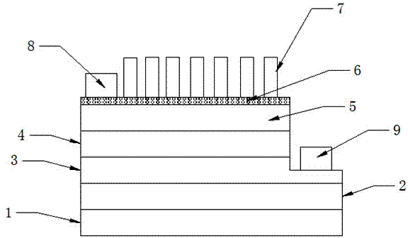
[0025] Example 1: Such as figure 1 As shown, an LED chip with a composite transparent conductive electrode is prepared by MOCVD on Al 2 o 3 Or GaN substrate (1) sequentially grow gallium nitride buffer layer (2), N-GaN layer (3), quantum well layer (4), P-GaN layer (5); coating on the P-GaN layer A layer of photoresist, followed by exposure and development, and one side of the P-GaN layer is etched to the N-GaN layer by ICP (reactive ion etching method) (3); firstly, graphene oxide and polymethacrylate The ester (PMMA) material is uniformly mixed and coated on the substrate wafer, so that the graphene oxide can be tightly attached to the wafer in the reactor without being blown away by the carrier gas or protective gas, and PMMA Also play the mechanical support effect to reaction product-graphene; 2 is the carrier gas, N 2 In order to protect the gas, a graphene layered film (6) is obtained by chemical vapor deposition; the layered film (6) prepared in the above steps is...

Embodiment 2

[0026] Example 2: Such as figure 1 As shown, an LED chip with a composite transparent conductive electrode is prepared by MOCVD on Al 2 o 3Or GaN substrate (1) sequentially grow gallium nitride buffer layer (2), N-GaN layer (3), quantum well layer (4), P-GaN layer (5); coating on the P-GaN layer A layer of photoresist, followed by exposure and development, and one side of the P-GaN layer is etched to the N-GaN layer by ICP (reactive ion etching method) (3); firstly, the graphene and polymethyl methacrylate (PMMA) materials are uniformly mixed and coated on the substrate wafer, so that graphene can be tightly attached to the wafer in the reactor without being blown away by the carrier gas or protective gas, and PMMA also acts To the mechanical support of the reaction product-graphene; the above-mentioned material is placed in a medium temperature tube furnace, with H 2 is the carrier gas, N 2 In order to protect the gas, a graphene layered film (6) is obtained by chemical...

Embodiment 3

[0027] Example 3: Such as figure 1 As shown, an LED chip with a composite transparent conductive electrode is prepared by MOCVD on Al 2 o 3 Or GaN substrate (1) sequentially grow gallium nitride buffer layer (2), N-GaN layer (3), quantum well layer (4), P-GaN layer (5); coating on the P-GaN layer A layer of photoresist, followed by exposure and development, and one side of the P-GaN layer is etched to the N-GaN layer by ICP (reactive ion etching method) (3); firstly, graphene oxide and polymethacrylate The ester (PMMA) material is uniformly mixed and coated on the substrate wafer, so that the graphene oxide can be tightly attached to the wafer in the reactor without being blown away by the carrier gas or protective gas, and PMMA Also play the mechanical support effect to reaction product-graphene; 2 is the carrier gas, N 2 In order to protect the gas, a graphene layered film (6) is obtained by chemical vapor deposition; the layered film (6) prepared in the above steps is...


PUM

PropertyMeasurementUnit
thicknessaaaaaaaaaa
thicknessaaaaaaaaaa

Abstract

The invention discloses an LED (Light Emitting Diode) chip for a composite transparent conducting electrode. The LED chip comprises a gallium nitride buffer layer, an N-GaN layer, a quantum well layer, a P-GaN layer and a composite transparent electrode layer which grow on a substrate in sequence. The LED chip is characterized in that an n-type electrode is manufactured on the N-GaN layer; a p-type electrode is manufactured on a graphene layer of the composite transparent electrode layer; the composite transparent electrode layer is formed by compounding a graphene laminar film and ZnO nanorods growing on the graphene laminar film. The invention also discloses a manufacturing method of the chip. The graphene laminar film/ZnO nanorod compounded transparent electrode layer formed by the manufacturing method has the advantages of capability of preventing cracking and good light transmittance performance and is easy to process, so that the contact performance, the current expansion performance and the transmissivity of the chip are greatly improved, and the production cost of the subsequent chip technology can be greatly reduced.

Description

technical field [0001] The invention relates to the technical field of LED chips, in particular to an LED chip with composite transparent conductive electrodes and a manufacturing method thereof. Background technique [0002] As a new type of wide-bandgap semiconductor material, ZnO has the same structure and similar photoelectric properties as GaN, and even surpasses GaN in terms of exciton emission performance, making it an excellent candidate for high-efficiency LEDs and UV wavelength LEDs By. ZnO has high transmittance in the visible light spectrum, and its electrical conductivity is close to that of metal thin films, and very close to ITO thin films. The doped or composite ZnO transparent conductive thin films have electrical and optical properties comparable to ITO thin films. In addition, compared with ITO, ZnO has the advantages of non-toxic, non-polluting, abundant raw materials, and low cost. The doped ZnO transparent conductive film has electrical and optical pro...

Claims


Application Information

Patent Timeline
Patent Type & Authority Applications(China)
IPC IPC(8): H01L33/38H01L33/42H01L33/00
CPCH01L33/005H01L33/38H01L33/42H01L2933/0016
Inventor 李方芳郝锐许德裕王波罗长得易翰翔刘洋
Owner GUANGDONG DELI PHOTOELECTRIC
Why Eureka
Try Eureka