Planar indium gallium arsenic light-sensitive chip with surface passivation improved and manufacturing method

An indium gallium arsenic, planar technology, applied in the fields of final product manufacturing, sustainable manufacturing/processing, electrical components, etc., can solve the problems of reduced surface passivation, InP surface oxidation, and epitaxial material surface damage, etc., to achieve enhanced passivation chemical effect

Active Publication Date: 2015-04-22
无锡中科德芯感知科技有限公司
View PDF3 Cites 5 Cited by
  • Summary
  • Abstract
  • Description
  • Claims
  • Application Information

AI Technical Summary

Problems solved by technology

[0010] In the manufacturing process of the existing planar InGaAs detector chip, the epitaxial material not only has to be exposed to the air, but also has to go through high-temperature processes such as diffusion. On the one hand, the surface passivation effect of the silicon nitride diffusion mask will be reduced. On the other hand, the InP surface exposed by the mask window will also be severely oxidized
In ad

Method used


Image

  • Planar indium gallium arsenic light-sensitive chip with surface passivation improved and manufacturing method
  • Planar indium gallium arsenic light-sensitive chip with surface passivation improved and manufacturing method

Examples


Embodiment Construction

[0045] The specific implementation method of the present invention will be described in detail below in conjunction with the accompanying drawings.

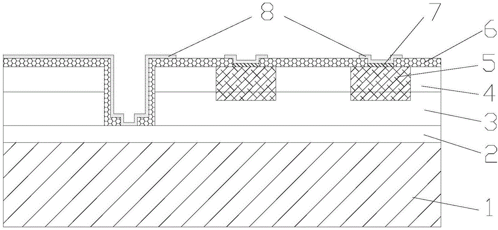
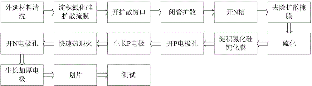
[0046] as attached figure 1 As shown, the epitaxial wafer used in this embodiment adopts metal-organic chemical vapor deposition (MOCVD) technology, and on a semi-insulating InP substrate 1 with a thickness of 350 μm, an N-type InP layer 2 with a thickness of 0.5 μm is sequentially grown. Fluor concentration>2×10 18 cm -3 ; InGaAs intrinsic absorption layer 3 with a thickness of 2.5 μm and a carrier concentration of 5×10 16 cm -3 ; An N-type InP cap layer 4 with a thickness of 1 μm and a carrier concentration of 5×10 16 cm -3 . The preparation process of the planar InGaAs infrared detector chip in this embodiment is based on the existing process, after the closed-tube diffusion, the process of adding nitrogen atmosphere heat treatment; before depositing the silicon nitride passivation film, introducing The process of remov...


PUM


Abstract

The invention discloses a planar indium gallium arsenic light-sensitive chip with surface passivation improved and a manufacturing method. According to the structure of the planar indium gallium arsenic light-sensitive chip, an N-type InP layer, an indium gallium arsenic intrinsic absorption layer, an N-type InP cap layer, a SiNx passivation layer, a P-electrode and a thickened electrode (8) are grown on a semi-insulating InP substrate in sequence. The manufacturing process is improved on the basis of an original process, and comprises removal and vulcanization of a diffusion mask and silicon nitride passive film growing through an inductive coupling plasma chemical vapor deposition (ICPCVD) technology. The planar indium gallium arsenic light-sensitive chip with surface passivation improved and the manufacturing method have the advantages the passivation layer of the chip is even in structure; the surface state density of a device is effectively reduced, and the surface can be prevented from being oxidized again through a vulcanization film formed on the surface; damage of the process to the surface of materials is small, the film is compact and is in stress fit with the substrate, the element bonding state is good, and the passivaition effect is excellent.

Description

technical field [0001] The invention relates to the preparation technology of infrared detection devices, specifically a planar indium gallium arsenic photosensitive chip with improved surface passivation effect and its preparation method, which is suitable for preparing planar indium gallium arsenic detectors with high sensitivity and high reliability . Background technique [0002] InGaAs short-wave infrared detectors can achieve good performance at room temperature, which makes them have broad application prospects in civil, military and aerospace fields. Because the planar process brings lower damage to the preparation of the device, this makes the planar device have relatively excellent performance, and has strong competitiveness in realizing high performance, miniaturization, and low power consumption of the system. [0003] The cross-sectional structure of the planar InGaAs detector chip is shown in the attached figure 1 As shown, it consists of InP substrate 1, N-t...

Claims


Application Information

Patent Timeline
IPC IPC(8): H01L31/0216H01L31/18H01L31/101
CPCH01L31/0216H01L31/09H01L31/1844Y02P70/50
Inventor 曹高奇唐恒敬王云姬李雪邵秀梅程吉凤龚海梅
Owner 无锡中科德芯感知科技有限公司
Why Eureka
Try Eureka