Method for preparing surface-enhanced Raman spectrum substrate and substrate prepared by using method

A surface-enhanced Raman and spectroscopy technology, applied in the process of producing decorative surface effects, Raman scattering, manufacturing microstructure devices, etc., can solve the problem of not being able to provide sensitivity and stability at the same time, and achieve good sensitivity and stability. High stability, stable performance and high repeatability

Inactive Publication Date: 2015-05-20
SHANGHAI INST OF APPLIED PHYSICS - CHINESE ACAD OF SCI
View PDF4 Cites 24 Cited by
  • Summary
  • Abstract
  • Description
  • Claims
  • Application Information

AI Technical Summary

Problems solved by technology

[0005] In order to solve the problem that the above-mentioned prior art cannot provide good sensitivity and stability at the same t

Method used


Image

  • Method for preparing surface-enhanced Raman spectrum substrate and substrate prepared by using method
  • Method for preparing surface-enhanced Raman spectrum substrate and substrate prepared by using method
  • Method for preparing surface-enhanced Raman spectrum substrate and substrate prepared by using method

Examples


Embodiment 1

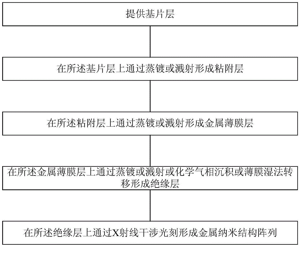
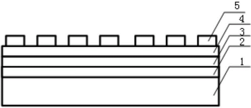
[0031] Put the 2-inch silicon substrate into acetone and anhydrous alcohol successively, and carry out surface cleaning with ultrasonic wave (ultrasonic frequency is 50Hz), after drying, use oxygen plasma bombardment (oxygen flow rate is 15sccm), plasma power is 100W , remove the organic matter on the surface of the substrate as the substrate layer 1;

[0032]Chromium was deposited on the substrate layer 1 with a thickness of 2 nm as the adhesion layer 2 by electron beam evaporation, and the pressure was 1×10 -7 Torr, power is 145W, deposition rate is 0.04nm / s;

[0033] A gold film with a thickness of 50 nm was deposited on the adhesion layer 2 by electron beam evaporation as the metal film layer 3, and the pressure was 1×10 -7 Torr, power is 115W, deposition rate is 0.12nm / s;

[0034] Deposition of SiO with a thickness of 10 nm on the metal thin film layer 3 by magnetron sputtering 2 As insulating layer 4, the pressure is 5×10 -3 Torr, power is 150W, deposition rate is 0....

Embodiment 2

[0039] Put the 2-inch silicon substrate into acetone and anhydrous alcohol successively, and carry out surface cleaning with ultrasonic wave (ultrasonic frequency is 50Hz), after drying, use oxygen plasma bombardment (oxygen flow rate is 10sccm), plasma power is 30W , remove the organic matter on the surface of the substrate as the substrate layer 1;

[0040] Using magnetron sputtering, 2nm thickness of titanium was evaporated on the substrate layer 1 as the adhesion layer 2, and the pressure was 5×10 -2 Torr, power is 100W, deposition rate is 0.24nm / s;

[0041] A silver thin film with a thickness of 50 nm was deposited on the adhesion layer 2 by magnetron sputtering as the metal thin film layer 3, and the pressure was 2.5×10 -3 Torr, power is 100W, deposition rate is 0.42nm / s;

[0042] 1.8 nm thick TiO deposited on metal thin film layer 3 by chemical vapor deposition 2 As the insulating layer 4, the temperature is 150°C, the flow rate is 20sccm, the time is 30 minutes, and...

Embodiment 3

[0046] Put the 2-inch silicon substrate into acetone and anhydrous alcohol successively, and carry out surface cleaning with ultrasonic wave (ultrasonic frequency is 50Hz), after drying, use oxygen plasma bombardment (oxygen flow rate is 10sccm), plasma power is 50W , remove the organic matter on the surface of the substrate as the substrate layer 1;

[0047] Chromium was deposited on the substrate layer 1 with a thickness of 2 nm as the adhesion layer 2 by electron beam evaporation, and the pressure was 1×10 -7 Torr, power is 145W, deposition rate is 0.14nm / s;

[0048] A gold film with a thickness of 100 nm was deposited on the adhesion layer 2 by electron beam evaporation as the metal film layer 3, and the pressure was 1×10 -7 Torr, power is 115W, deposition rate is 0.14nm / s;

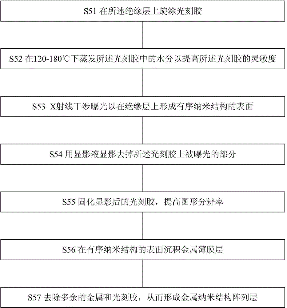
[0049] Using thin film wet transfer method to deposit graphene as insulating layer 4 on metal thin film layer 3, including (1) spin-coating a layer of 200nm PMMA on graphene surface as protective la...


PUM


Abstract

The invention provides a method for preparing a surface-enhanced Raman spectrum substrate. The method comprises the following steps: preparing a substrate layer; forming an adhesion layer on the substrate layer by virtue of evaporation plating or sputtering; forming a metal thin film layer on the adhesion layer by virtue of evaporation plating or sputtering; forming an insulating layer on the metal thin film layer by virtue of evaporation plating or sputtering or chemical vapor deposition or thin film wet-process transfer; forming a metal nano-structure array layer on the insulating layer by virtue of X-ray interference lithography, wherein the X-ray interference lithography comprises photoresist spin-coating; evaporating moisture in a photoresist at 120-180 DEG C; performing X-ray interference exposure; performing development by using a developing solution; curing the developed photoresist; depositing the metal thin film layer on the surface of an ordered nanostructure; and removing excess metals and photoresists. The invention also relates to a surface-enhanced Raman spectrum substrate comprising the substrate layer, the adhesion layer, the metal thin film layer, the insulating layer and the metal nano-structure array layer. The surface-enhanced Raman spectrum substrate prepared by using the method disclosed by the invention has both good sensitivity and stability.

Description

technical field [0001] The present invention relates to the technical field of surface-enhanced Raman spectroscopy, and more particularly to a method for preparing a surface-enhanced Raman spectroscopy substrate and its substrate. Background technique [0002] Raman spectroscopy is a spectroscopic method used to study effective molecular vibrations and is an important molecular spectroscopy technique. According to the different Raman spectral characteristics of different substance molecules because of their different chemical compositions and structures, researchers can obtain molecular information from Raman spectroscopy to identify and detect different substances. Raman scattering is a kind of inelastic scattering, and its intensity is much weaker than that of Rayleigh scattering, so conventional Raman spectroscopy is very insensitive in analyzing the valence state and composition of substances. [0003] Surface-enhanced Raman scattering (SERS) technology can simultaneous...

Claims


Application Information

Patent Timeline
IPC IPC(8): G01N21/65B81C1/00B82Y40/00
Inventor 刘星邰仁忠吴衍青杨树敏赵俊王连升薛超凡
Owner SHANGHAI INST OF APPLIED PHYSICS - CHINESE ACAD OF SCI
Why Eureka
Try Eureka