Transient voltage suppression diode array chip according to mesa trench isolation method and production technology thereof

A technology of transient voltage suppression and diode array, which is applied in semiconductor/solid-state device manufacturing, circuits, electrical components, etc., can solve the problems of vulnerable devices to be protected, large voltage resilience, diode breakdown, etc., to achieve protection from damage, reduce leakage current, and protect the device

Active Publication Date: 2015-07-29
SUZHOU QILAN POWER ELECTRONICS
View PDF6 Cites 8 Cited by
  • Summary
  • Abstract
  • Description
  • Claims
  • Application Information

AI Technical Summary

Problems solved by technology

[0003] At present, planar technology is mostly used in the industry to manufacture transient voltage suppression diode arrays, and there is a technical defect: 1) high cost and complicated process; 2) PN junctions are formed on the surface and protected by silicon oxide dielectric films, which are susceptible...

Method used


Image

  • Transient voltage suppression diode array chip according to mesa trench isolation method and production technology thereof
  • Transient voltage suppression diode array chip according to mesa trench isolation method and production technology thereof
  • Transient voltage suppression diode array chip according to mesa trench isolation method and production technology thereof

Examples


Embodiment Construction

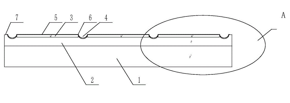
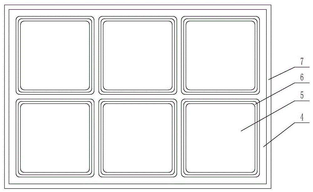
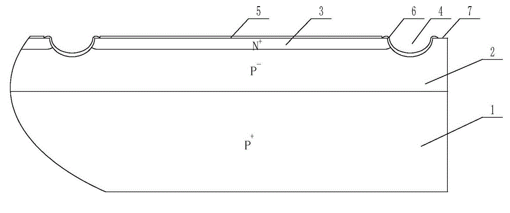
[0036] The chip of the transient voltage suppression diode array with mesa trench isolation method according to the present invention and its production process will be described in further detail below through specific embodiments.

[0037] Such as Figure 5 As shown, a production process of a mesa trench isolation method transient voltage suppression diode array chip includes the following steps:

[0038] 1) Cleaning before oxidation: through electronic cleaning agent SC 2 , Deionized water ultrasonic cleaning and other processes, chemically treat the surface of the silicon wafer to obtain a clean original P-type silicon wafer with a resistivity of 0.005~0.006Ω.cm;

[0039] 2) Oxidation: the cleaned silicon wafer is grown on both sides in an oxidation furnace at 1100~1200℃ as a mask, the thickness of the oxide film is 1.5μm~2μm;

[0040] 3) Removal of single-sided oxide film: Coat a layer of photoresist on one side of the oxidized silicon wafer, and use ammonium fluoride etching solu...


PUM

PropertyMeasurementUnit
Resistivityaaaaaaaaaa
Thicknessaaaaaaaaaa

Abstract

The invention relates to a transient voltage suppression diode array chip according to a mesa trench isolation method and a manufacturing technology thereof. A method that a mesa isolation trench is manufactured on an N+ surface by adopting the mesa technology is adopted so that multiple transient suppression diodes can be thoroughly separated, surface breakdown can be changed into body breakdown and thus reliability of the diodes is increased; a method that P+ junctions are formed by coating a liquid boron source through deep junction diffusion is adopted so that an epitaxial wafer can be substituted for chip manufacturing, diffused junction depth is flat and uniform, and width of a substrate passive region is controllable without limitation of width of an epitaxial layer; a mesa protective layer is formed by adopting glass powder electrophoresis so that mechanical damage resistant capacity of the diode array can be enhanced and anti-surge capacity of the diode array can also be enhanced; and a glass burning method with chlorine is adopted so that width of a diode PN-junction depletion layer can be increased, junction capacitance can be reduced, surge voltage of the diodes is enabled to be rapidly clamped to a safe voltage range, and thus subsequent digital circuits can be protected from being damaged.

Description

Technical field [0001] The present invention relates to the technical field of transient voltage suppression diode production, in particular to a mesa trench isolation method transient voltage suppression diode array (TVS array) chip and its production process. Background technique [0002] With the development of electronic technology, more and more devices and applications require a transient voltage suppression diode array structure to provide electrostatic discharge (ESD) protection. The transient voltage suppression diode array is usually several or even dozens of transients. Suppressor diodes are integrated in a chip to form an array of common anode transient suppression diode modules, which are mostly used to prevent the circuit from being damaged by sudden overvoltage. Typical applications include universal serial bus (USB) power and data lines Protection, digital image interface, high-speed Ethernet, notebook computers, monitors, etc., especially for high-bandwidth data ...

Claims


Application Information

Patent Timeline
IPC IPC(8): H01L21/329H01L21/228H01L21/265
CPCH01L21/228H01L21/265H01L21/26506H01L29/66136H01L29/66143
Inventor 丛培金范玉丰丛济洲
Owner SUZHOU QILAN POWER ELECTRONICS
Why Eureka
Try Eureka