GaN E/D integrated device production method based on two-step oxidation method
A technology of secondary oxidation and integrated devices, which is applied in semiconductor/solid-state device manufacturing, electric solid-state devices, semiconductor devices, etc. Process consistency and controllability are not high, etching damage reduces device saturation current, etc., to achieve high process stability and consistency, low interface state density, and good on-chip consistency.
- Summary
- Abstract
- Description
- Claims
- Application Information
AI Technical Summary
Problems solved by technology
Method used
Image
Examples
preparation example Construction
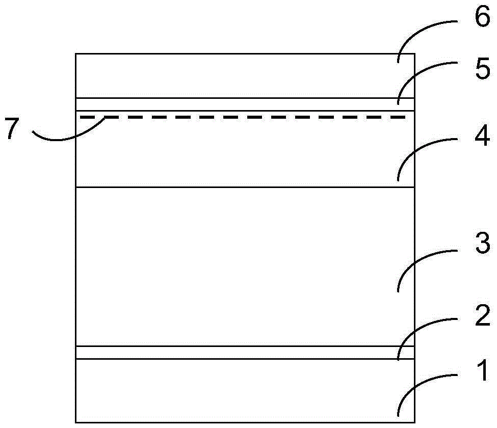
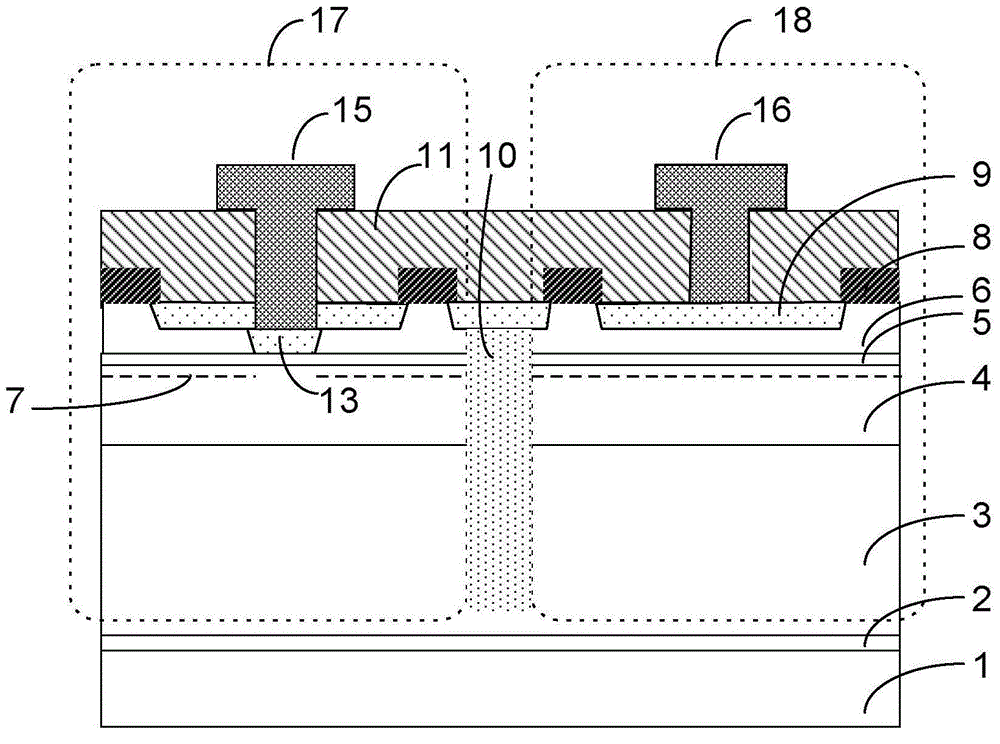
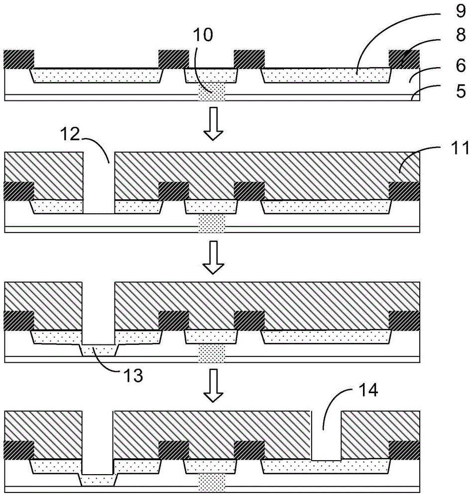
[0026] Such as Figure 1~3 As shown, a GaN E / D integrated device preparation method based on the secondary oxidation method, the preparation steps include the following in sequence:
[0027] a) On the substrate 1, the nucleation layer 2, the AlyGa1-yN buffer layer 3, the GaN channel layer 4, the AlN insertion layer 5, and the barrier layer 6 are sequentially grown to form a GaN HEMT heterostructure, and the heterointerface forms a two-dimensional Electron Gas 7;
[0028] b) After the conventional ohmic metal electrode 8 is completed, the oxygen plasma treatment method is used for the first oxidation to consume part of the barrier layer 6 to reduce its thickness to half of the original, and at the same time the first layer of oxidized medium 9 is formed on the surface; The two-dimensional electron gas 7 is still retained in the time channel;
[0029] c) Perform device isolation 10, make a mask 11, open holes in the area 12 reserved for making the gate pin of the E-mode device...
Embodiment 1
[0034] An AlN nucleation layer 2 is grown on the SiC substrate, and then 1 μm GaN is grown as a buffer layer 3, 40nm undoped GaN is used as a channel layer 4, a 1.5nm AlN insertion layer 5 is finally covered with a 6nm undoped Al0.72In0.18N potential Barrier layer 5, in which the concentration of two-dimensional electron gas 7 is 1.87×10 13cm -2 , forming AlInN / AlN / GaN heterostructure materials for E / D integration. After the conventional ohmic metal electrode 8 is completed, the first oxidation treatment is carried out. The oxidation condition can consume the 3nm Al0.72 In0.18N barrier layer 5 to form the first layer of oxide medium 9, and then adopt the method of B ion implantation Isolate 10, make a mask 11, open a window by photolithography in the area 12 reserved for making the gate pin of the E-mode device, remove the gate pin dielectric 9 of the E-mode device, and then perform the second oxidation. The oxidation conditions are the same as the first oxidation conditions ...
Embodiment 2
[0036] An AlN nucleation layer 2 is grown on the SiC substrate, and then 1 μm Al0.08Ga0.92N is grown as the buffer layer 3, 20nm undoped GaN is grown as the channel layer 4, 2nm AlN is inserted into the layer 5, and finally 4nm undoped Al0. 5Ga0.5N barrier layer 5, in which the concentration of two-dimensional electron gas 7 is 1.32×10 13 cm -2 , forming AlGaN / AlN / GaN heterostructure materials for E / D integration. After the conventional ohmic metal electrode 8 is completed, the first oxidation treatment is carried out. The oxidation condition can consume the 2nm Al0.5Ga0.5N barrier layer 5 to form the first layer of oxide medium 9, and then use B ion implantation method for isolation 10. Make a mask 11, open a window by photolithography in the area 12 reserved for making the gate pin of the E-mode device, remove the gate pin dielectric 9 of the E-mode device, and then perform the second oxidation. The oxidation condition is completely the same as the first oxidation condition...
PUM
 Abstract
Description
Claims
Application Information


