Solar battery with structure of oxide-metal multilayer film/silicon substrate
A technology for solar cells and oxide films, applied in the field of solar cells, can solve the problems of expensive equipment, high-risk chemicals in raw materials, etc., and achieve the effects of fewer manufacturing processes, reduction of Auger recombination and dead layers, and low cost
- Summary
- Abstract
- Description
- Claims
- Application Information
AI Technical Summary
Problems solved by technology
Method used
Image
Examples
Embodiment 1
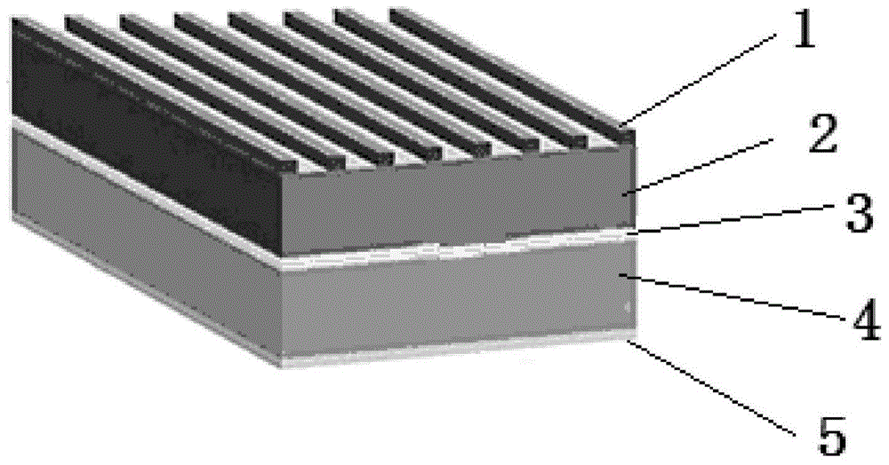
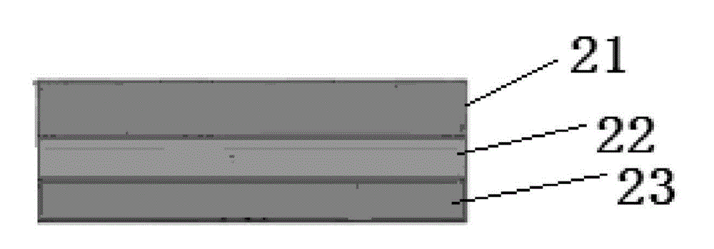
[0038] Such as figure 1As shown in , the structure provided in this embodiment is an oxide-metal multilayer film / silicon-based solar cell, and the structure of the solar cell includes from top to bottom: silver electrode 1, oxide-metal multilayer film 2, passivation layer 3, a silicon substrate 4 and an all-aluminum back electrode 5, the oxide-metal multilayer film 2 is composed of a first oxide film 21, a metal film 22 and a second oxide film 23, wherein the first oxide film 21 and the second oxide film 23 is MoO 3 film, the metal film 22 is an Ag film, and the passivation layer 3 is SiO 2 passivation layer.
[0039] Wherein the thickness of the first oxide film is 10-20 nm, the thickness of the metal film is 2-15 nm, and the thickness of the second oxide film is 30-50 nm.
[0040] The above structure is an oxide-metal multilayer film / silicon-based solar cell, which is prepared by the following method:
[0041] (1) Clean the n-type or p-type single crystal silicon wafer w...
Embodiment 2
[0048] The structure provided in this embodiment is an oxide-metal multilayer film / silicon-based solar cell. The difference from Embodiment 1 is that the passivation layer 3 is Al 2 o 3 passivation layer.
[0049] The above structure is an oxide-metal multilayer film / silicon-based solar cell, which is prepared by the following method:
[0050] (1) Clean the n-type or p-type single crystal silicon wafer with the RCA process, and then use atomic layer deposition (ALD) technology to deposit a layer of Al on the surface of the silicon wafer 2 o 3 Passivation layer, set the deposition temperature to 200°C, Al(TMA), N 2 、H 2 The pulse time of O is: 0.1s, 10s and 0.1s respectively, the flow rate is respectively: 150sccm, 150sccm and 200sccm, and 10-30 cycles are performed to deposit 1-3nm aluminum oxide on the surface of the silicon wafer;
[0051] (2) Then MoO is prepared on the surface of the passivation layer by a resistive thermal evaporation coating machine 3 Thin film, va...
Embodiment 3
[0056] The structure provided in this embodiment is an oxide-metal multilayer film / silicon-based solar cell. The difference from Embodiment 1 is that the passivation layer 3 is TiO 2 passivation layer.
[0057] The above structure is an oxide-metal multilayer film / silicon-based solar cell, which is prepared by the following method:
[0058] (1) Clean the n-type or p-type single crystal silicon wafer with the RCA process, and then use atomic layer deposition (ALD) technology to deposit a layer of TiO on the surface of the silicon wafer 2 Passivation layer, set the deposition temperature to 200-300°C, TiCl 4 , N 2 、H 2 The pulse time of O is: 1s, 3s and 1s respectively, the flow rate is respectively: 150sccm, 150sccm and 200sccm, carry out 10-30 cycles, and deposit 1-3nm titanium dioxide on the surface of the silicon wafer;
[0059] (2) Then MoO is prepared on the surface of the passivation layer by a resistive thermal evaporation coating machine 3 Thin film, vacuum degree ...
PUM
| Property | Measurement | Unit |
|---|---|---|
| Thickness | aaaaa | aaaaa |
| Thickness | aaaaa | aaaaa |
| Thickness | aaaaa | aaaaa |
Abstract
Description
Claims
Application Information


