Solar cell adopting metal transparent electrode and preparation of solar cell

A technology of solar cells and transparent electrodes, applied in circuits, photovoltaic power generation, electrical components, etc., can solve problems such as high cost, poor conductivity, poor flexibility, and harsh preparation conditions

Inactive Publication Date: 2015-09-23
HUANENG CLEAN ENERGY RES INST +1
View PDF6 Cites 10 Cited by
  • Summary
  • Abstract
  • Description
  • Claims
  • Application Information

AI Technical Summary

Problems solved by technology

At present, the commonly used transparent electrodes are FTO (fluorine-doped tin oxide), ITO (indium tin oxide), AZO (aluminum-doped zinc oxide), etc., this kind of transparent electrode of metal oxide semiconductor has a high light transmittance of about 90%. In addition to its advantages, its conductivity and flexibility are poor; in addition, its production mostly requires the use of high-energy-consuming preparation methods and corresponding equipment such as magnetron sputtering, atomic deposition, laser deposition, chemical vapor deposition, and molecular beam epitaxy. , high cost and harsh preparation conditions

Method used


Image

  • Solar cell adopting metal transparent electrode and preparation of solar cell
  • Solar cell adopting metal transparent electrode and preparation of solar cell
  • Solar cell adopting metal transparent electrode and preparation of solar cell

Examples


Embodiment 1

[0029] A solar cell using a metal transparent electrode, comprising: a metal counter electrode layer 112 , a metal transparent electrode layer 102 and an active perovskite layer 108 located between the metal counter electrode layer 112 and the metal transparent electrode layer 102 .

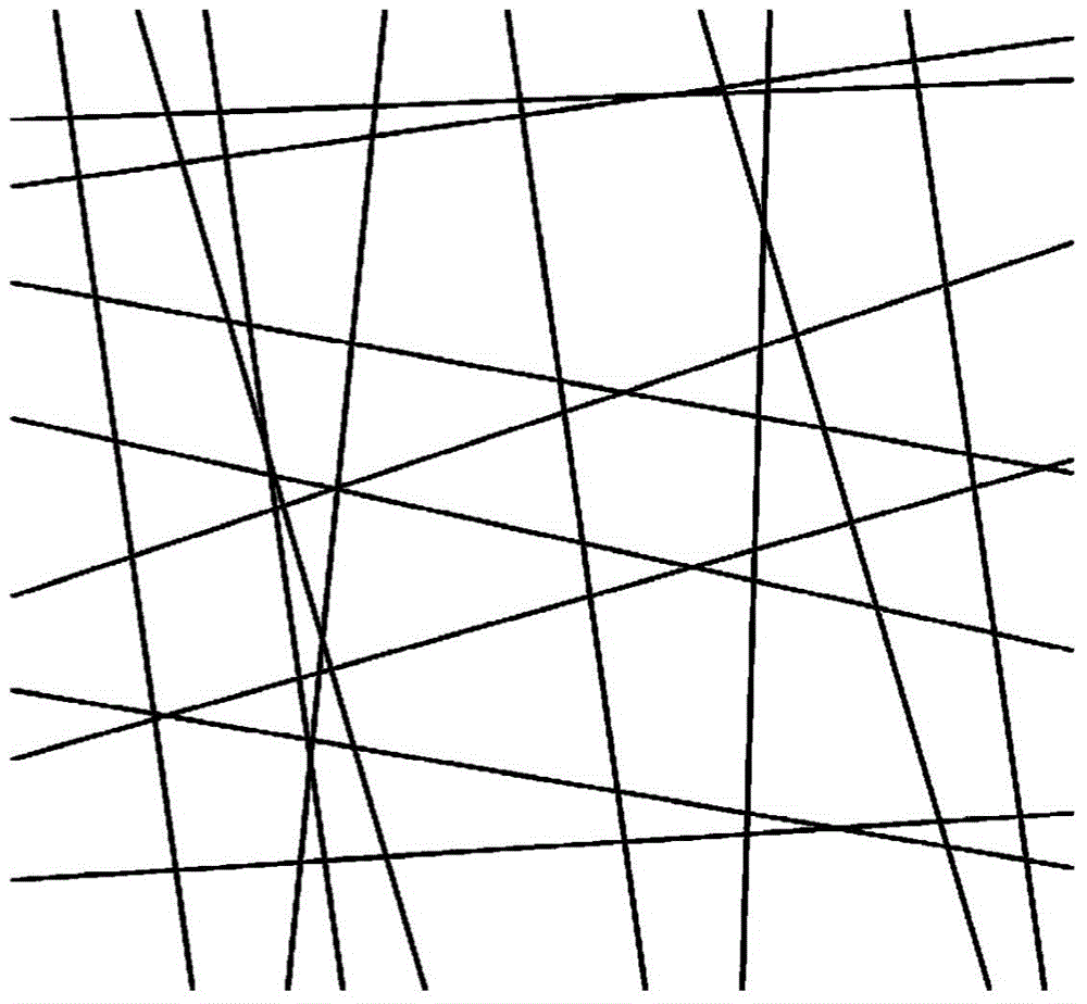
[0030] The metal transparent electrode layer 102 is a metal nanowire mesh conductive film, the metal is Cu, Fe, Ni, Ag, Au or Pt, etc., the diameter of the nanowire is 10-100nm, and the aspect ratio of the nanowire is more than 1000:1. Further, it can have a higher aspect ratio such as 10000:1 to ensure that it has better light transmission performance and certain electrical conductivity. The metal nanowires have a random network structure, such as image 3 As shown, each black line represents a metal nanowire with a diameter of 10-100 nm. If photolithography, nano-etching, atomic deposition, vapor deposition, magnetron sputtering, thermal evaporation, etc. are used, the corresponding template c...

Embodiment 2

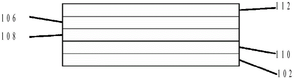
[0038] like figure 1As shown, on the basis of Embodiment 1, an electron transport layer 106 is provided between the metal counter electrode layer 112 and the active perovskite layer 108, and a hole transport layer 110 is provided between the metal transparent electrode layer 102 and the active perovskite layer 108. .

[0039] The electron transport layer 106 is usually made of mesoporous titanium dioxide, which is prepared by annealing and sintering after preparing a sol of mesoscopic particles by a sol-gel method. A fullerene-based electron transport layer material may also be used instead. The thickness of this layer is 100-2000nm.

[0040] The hole transport layer 110 is characterized by organic and inorganic materials that match the energy level of the perovskite active material, such as cuprous iodide, PEDOT:PSS, polyparaphenylene vinylene, polythiophene, polysilane, Triphenylmethanes, triarylamines, hydrazones, pyrazolines, azoles, carbazoles, butadiene, etc., the thi...

Embodiment 3

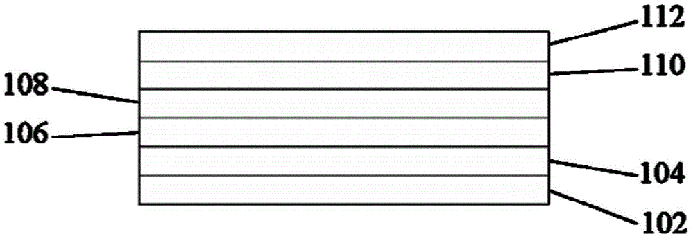
[0048] like figure 2 As shown, on the basis of Embodiment 1, a hole transport layer 110 is provided between the metal counter electrode layer 112 and the active perovskite layer 108, and an electron transport layer 106 or A dense semiconductor layer 104 is disposed between the porous support layer, the electron transport layer 106 or the porous support layer and the metal transparent electrode layer 102 .

[0049] The semiconductor dense layer 104 is usually titanium dioxide or zinc oxide, and its thickness is 20-150 nm.

[0050] If the semiconductor dense layer 104 and the hole transport layer 110 are not provided, the process can be simplified and the cost can be reduced, but the cell efficiency obtained is relatively low.

[0051] The principle of this embodiment:

[0052] 1. Metal transparent electrode layer 102: collects and conducts the electrons conducted by the semiconductor dense layer 104 (if used) or the electron transport layer 106 (if the material layer 104 is ...


PUM

PropertyMeasurementUnit
thicknessaaaaaaaaaa
thicknessaaaaaaaaaa
thicknessaaaaaaaaaa

Abstract

A solar cell adopting a metal transparent electrode comprises a metal counter electrode layer, a metal transparent electrode layer and an active calcium titanium ore bed positioned between the metal counter electrode layer and the metal transparent electrode layer; an electronic transmission layer or a hole transmission layer can be arranged between the metal counter electrode layer and the active calcium titanium ore bed; a hole transmission layer or an electronic transmission layer is arranged between the metal transparent electrode layer and the active calcium titanium ore bed; and a semiconductor compact layer can be further arranged between the electronic transmission layer and the metal transparent electrode layer. The solar cell adopts a metal nanowire net conductive thin film with high light transparency as the metal transparent electrode layer, wherein the conductivity, the light transparency and the flexibility of the metal nanowire net conductive thin film are greatly superior to those of semiconductor metallic oxide.

Description

technical field [0001] The invention belongs to the technical field of design and preparation of thin-film solar cell devices, in particular to a solar cell using metal transparent electrodes and its preparation. Background technique [0002] With the depletion of fossil energy and the high environmental costs brought about by its use, the development and utilization of renewable clean energy has attracted extensive attention. Solar photovoltaic power generation technology and products have been growing rapidly around the world, becoming the most potential clean energy. Perovskite solar cells discovered in recent years have attracted much attention due to their high conversion efficiency, low cost, environmental friendliness, and flexible productization. [0003] The transparent electrode is one of the key parts in the perovskite solar cell structure, which plays a role in conducting the photocurrent generated by the solar cell to the external circuit. Transparent electrod...

Claims


Application Information

Patent Timeline
Patent Type & Authority Applications(China)
IPC IPC(8): H01L51/42H01L51/44H01L51/48
CPCH10K71/12H10K30/151H10K30/82Y02E10/549Y02P70/50
Inventor 秦校军赵志国王一丹邬俊波
Owner HUANENG CLEAN ENERGY RES INST
Why Eureka
Try Eureka