Organic electroluminescent device and preparation method thereof
An electroluminescent device and luminescent technology, which is applied in the direction of electric solid-state devices, semiconductor/solid-state device manufacturing, electrical components, etc., can solve the problem of low starting voltage of organic electroluminescent devices, and achieve improved electron transmission efficiency and service life No effect, the effect of reducing the quenching phenomenon
- Summary
- Abstract
- Description
- Claims
- Application Information
AI Technical Summary
Problems solved by technology
Method used
Image
Examples
Embodiment 1
[0049] A method for preparing an organic electroluminescent device, comprising the following steps:
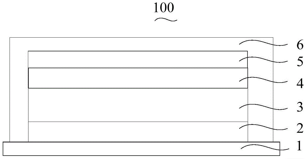
[0050] (1) Provide ITO conductive glass as the conductive anode 1 and clean it. The square resistance of the ITO conductive glass is 5Ω / □; the degree of vacuum is 1×10 -5 In the vacuum coating system of Pa, the hole transport layer 2 is prepared by vacuum evaporation on the surface of ITO conductive glass; the material of the hole transport layer is a mixed material formed by F4-TCNQ and NPB in a mass ratio of 1:100 , the thickness of the hole transport layer is 20nm, wherein the evaporation rate of F4-TCNQ is 0.01nm / s, and the evaporation rate of NPB is 1nm / s;
[0051] In a vacuum of 1×10 -5 In the vacuum coating system of Pa, the luminescent layer 3 is prepared by vacuum evaporation on the surface of the hole transport layer. The material of the luminescent layer is DMQA, the thickness of the luminescent layer is 10nm, and the evaporation rate is 0.1nm / s;
[0052] (2) In a...
Embodiment 2
[0060] (1) Provide ITO conductive glass as the anode and clean it. The square resistance of the ITO conductive glass is 100Ω / □; the vacuum degree is 1×10 -3 In Pa's vacuum coating system, the hole transport layer is prepared by vacuum evaporation on the surface of ITO conductive glass; the material of the hole transport layer is a mixture of F6-TNAP and MeO-TPD with a mass ratio of 10:100. Materials, the thickness of the hole transport layer is 60nm, the evaporation rate of F6-TNAP is 0.05nm / s, and the evaporation rate of MeO-TPD is 0.5nm / s.
[0061] In a vacuum of 1×10 -3 In Pa's vacuum coating system, the light-emitting layer is prepared by vacuum evaporation on the surface of the hole transport layer. The material of the light-emitting layer is C545T, the thickness of the light-emitting layer is 30nm, and the evaporation speed is 0.5nm / s;
[0062] (2) In a vacuum of 1×10 -3 In the vacuum coating system of Pa, the electron transport layer is prepared by vacuum evaporation ...
Embodiment 3
[0070] A method for preparing an organic electroluminescent device, comprising the following steps:
[0071] (1) Provide ITO conductive glass as the anode and clean it. The square resistance of the ITO conductive glass is 50Ω / □; the vacuum degree is 1×10 -4 In the vacuum coating system of Pa, the hole transport layer is prepared by vacuum evaporation on the surface of ITO conductive glass; the material of the hole transport layer is a mixed material formed by F2-HCNQ and TPD in a mass ratio of 5:100, The thickness of the hole transport layer is 40nm, the evaporation rate of F2-HCNQ is 0.01nm / s, and the evaporation rate of TPD is 0.2nm / s.
[0072] In a vacuum of 1×10 -4 In Pa's vacuum coating system, the luminescent layer is prepared by vacuum evaporation on the surface of the hole transport layer. The material of the luminescent layer is Rubrene, the thickness of the luminescent layer is 15nm, and the evaporation rate is 0.2nm / s;
[0073] (2) In a vacuum of 1×10 -4In the va...
PUM
 Abstract
Description
Claims
Application Information
 - R&D
- Intellectual Property
- Life Sciences
- Materials
- Tech Scout
- Unparalleled Data Quality
- Higher Quality Content
- 60% Fewer Hallucinations
Browse by: Latest US Patents, China's latest patents, Technical Efficacy Thesaurus, Application Domain, Technology Topic, Popular Technical Reports.
© 2025 PatSnap. All rights reserved.Legal|Privacy policy|Modern Slavery Act Transparency Statement|Sitemap|About US| Contact US: help@patsnap.com


