Wet chemical etching method for preparing large-area and flexible ultra-thin monocrystalline silicon wafers

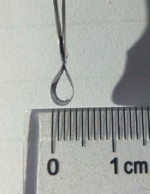
A single crystal silicon wafer, wet chemical technology, used in semiconductor/solid-state device manufacturing, electrical components, circuits, etc., can solve the problems of high equipment requirements, easy cracking and damage, brittleness and instability, and achieve high quality and size of finished products. Unlimited, thickness-controlled effects

Active Publication Date: 2015-11-11
NORTH CHINA ELECTRIC POWER UNIV (BAODING)
View PDF4 Cites 3 Cited by
  • Summary
  • Abstract
  • Description
  • Claims
  • Application Information

AI Technical Summary

Problems solved by technology

When the thickness is less than 50mm, it shows strong brittleness and instability, and is easily broken and damaged during traditional processing and transfer.
In addition to failing to meet the thinning requirements, the traditional thinning process is cumbersome an

Method used


Image

  • Wet chemical etching method for preparing large-area and flexible ultra-thin monocrystalline silicon wafers
  • Wet chemical etching method for preparing large-area and flexible ultra-thin monocrystalline silicon wafers

Examples


Embodiment 1

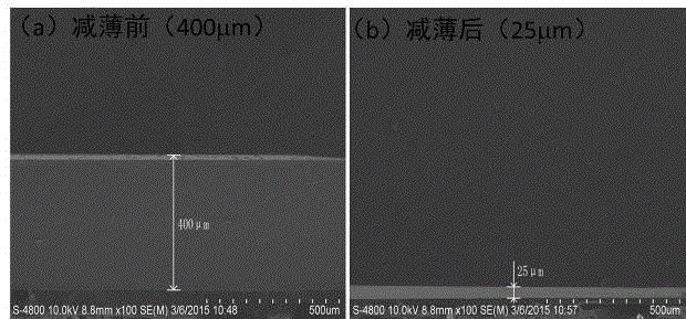
[0023] 1. Use N (100) double-sided polished single-crystal silicon wafers with a resistivity of 1~5W?cm, and ultrasonically clean them in acetone, absolute ethanol, and deionized water for 5 minutes each; rinse with deionized water after each ultrasonic wave 2 minutes; then soak in hydrofluoric acid with a mass percentage concentration of 5% for 5 minutes at room temperature; rinse with deionized water with a resistivity above 18W?cm for 2 minutes, and vacuum dry;

[0024] 2. Use solid potassium hydroxide, isopropanol and deionized water with a resistivity above 18W?cm to prepare a mixed solution (hereinafter referred to as thinning solution) with the following concentration characteristics: the mass percentage concentration of potassium hydroxide is 45% , the mass percentage concentration of isopropanol is 12%; stir on a magnetic stirrer for 10-20 minutes to promote the full dissolution of potassium hydroxide and make the solution evenly mixed; then put it into a water bath at...


PUM


Abstract

The invention discloses a wet chemical etching method for preparing large-area and flexible ultra-thin monocrystalline silicon wafers, and belongs to the field of semiconductor technology. According to the method, acetone, anhydrous ethanol, deionized water and hydrofluoric acid are adopted to treat a N(100) double-side-polished monocrystalline silicon wafer in advance, so that the surface of the silicon surface is cleaned. Potassium hydroxide, isopropanol and deionized water are uniformly mixed to prepare a reducer and the reducer is preheated in a water-bath. After that, the silicon wafer is well fixed and dipped in the reducer by a clamp. In this way, an ultra-thin wafer of a desired thickness can be obtained through controlling the reaction time and the reaction temperature, The surface of the silicon wafer is bright, flat, smooth and free of any obvious thinning defect, and appears the mirror-surface result. According to the technical scheme of the invention, the thinning process of silicon wafers is simplified by adopting the single-step method, and the characteristics of the wet etching technique in the low-temperature and normal-pressure condition are maintained. Silicon wafers with the thickness thereof smaller than 10 mm are obtained for the first time. Meanwhile, the application range of the wet silicon etching technique is expanded. Therefore, the method provides a novel idea and a novel technical means for the thinning process of silicon wafers.

Description

technical field [0001] The invention belongs to the technical field of semiconductors, and in particular relates to a method for preparing an ultra-thin single-crystal silicon chip used in the preparation of portable, ultra-thin, and fast heat dissipation semiconductor devices. In particular, it relates to a wet chemical etching method for preparing large-area flexible ultra-thin single-crystal silicon wafers. Background technique [0002] Silicon wafer thinning technology can achieve high production efficiency and simple thickness control, and was first applied to the treatment of silicon wafer cutting defects caused by inner circle slicing. With the rapid development of integrated circuit packaging technology, the miniaturization, portability and intelligence of electronic terminal equipment put forward higher requirements for the improvement of chip packaging structure and heat dissipation efficiency. The main building block for device stacking / 3D packaging. Nowadays, s...

Claims


Application Information

Patent Timeline
IPC IPC(8): H01L21/02
CPCH01L21/02019H01L21/02052
Inventor 李美成李瑞科陈杰威付鹏飞白帆黄睿
Owner NORTH CHINA ELECTRIC POWER UNIV (BAODING)
Why Eureka
Try Eureka