Visible light responsive nitride photocatalytic material and preparation method

A photocatalytic material, nitride light technology, applied in chemical instruments and methods, physical/chemical process catalysts, chemical/physical processes, etc., can solve the problem of low effective utilization of solar energy, reduce direct recombination rate, increase photo Effects of catalytic degradation efficiency and high photoelectric conversion efficiency

Inactive Publication Date: 2015-11-18
PEKING UNIV
View PDF2 Cites 3 Cited by
  • Summary
  • Abstract
  • Description
  • Claims
  • Application Information

AI Technical Summary

Problems solved by technology

[0003] In semiconductor photocatalysis research, TiO 2 It is widely used because of its high activity, safety and non-toxicity, stable chemical properties, and low cost. However, TiO 2 It can only be catalyzed in the ultraviolet range, and the effective utilization rate of solar energy is relatively low. Aiming at this bottleneck, some researchers began to turn their work to the design of new semiconductor photocatalysts with high efficiency and broad-spectrum response.

Method used


Image

  • Visible light responsive nitride photocatalytic material and preparation method
  • Visible light responsive nitride photocatalytic material and preparation method
  • Visible light responsive nitride photocatalytic material and preparation method

Examples


Embodiment Construction

[0033] Below in conjunction with accompanying drawing, the present invention will be further described through embodiment.

[0034] The preparation method of the visible light-responsive nitride photocatalytic material of this embodiment includes the following steps:

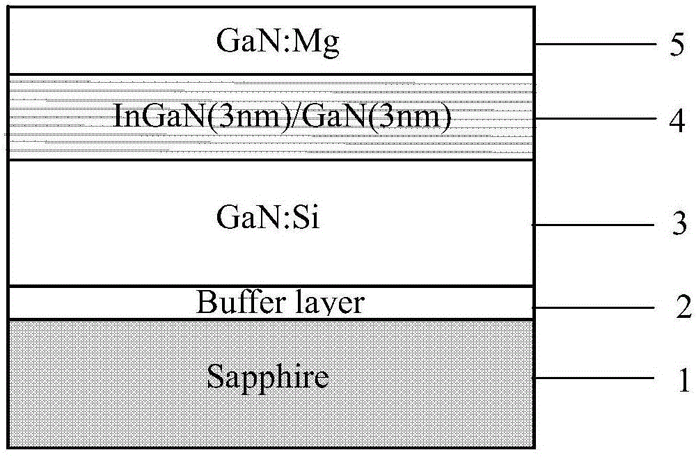
[0035]1) Use the MOCVD growth system of Aixtron Company, using trimethylgallium (TMGa), trimethylindium (TMIn), trimethylaluminum (TMAl) as the Group III source, ammonia (NH3) as the V group source, silane ( SiH4) as the n-type dopant source, dimagnesocene (Cp2Mg) as the p-type dopant source, grow a multi-layer PIN heterostructure nitride epitaxial film on the sapphire substrate, including the sapphire substrate 1, buffer layer (10nm ) 2, n-GaN layer (4μm) 3, InGaN (3nm) / GaN (3nm) multiple quantum wells (30 cycles) 4, p-GaN layer (200nm) 5, such as figure 1 shown.

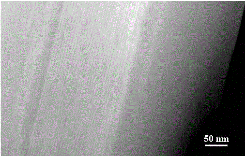
[0036] figure 2 High-angle annular dark field-scanning transmission electron micrograph (HAADF-STEM) shows that the MOCVD-grown InGaN / GaN MQW in...


PUM

PropertyMeasurementUnit
thicknessaaaaaaaaaa
thicknessaaaaaaaaaa
thicknessaaaaaaaaaa

Abstract

The invention discloses a visible light responsive nitride photocatalytic material and a preparation method. The preparation method comprises: growing multiple layers of GaN-based epitaxial thin films in PIN heterostructures on a sapphire substrate by adopting a MOCVD technology; using an InGaN/GaN multiple quantum well or a superlattice as a light absorption layer; and then transferring the GaN-based epitaxial thin films to a conductive substrate, and peeling the sapphire substrate to obtain the photocatalytic material. By adopting the InGaN/GaN multiple quantum well or a superlattice as the light absorption layer, the difficulty of growing thick InGaN by MOCVD is overcome; by doping the In component, the photocatalytic material has visible light responsiveness; photon-generated carriers can be effectively separated as a result of a built-in electric field in the PIN heterostructures, so that the material has a high photovoltaic conversion efficiency, and the catalytic activity of the material is greatly improved. The photocatalytic material illuminated by visible light shows excellent degradation activity to azo dyes such as methyl orange and the like, so that the photocatalytic material can be used as an electrode of a photoelectrochemical pool for degrading organic pollutants.

Description

technical field [0001] The invention relates to the technical field of inorganic semiconductor photocatalytic materials and environmental pollution control, in particular to a multi-quantum well or superlattice nitride photocatalytic material with high catalytic activity and a preparation method that can be used to degrade pollutants (dye) in response to visible light . Background technique [0002] With the rapid expansion of population and the rapid development of industry, energy issues and environmental pollution issues have become major challenges for mankind. A large amount of pollutant discharge, especially the large amount of water-soluble azo dyes such as methyl orange in the printing and dyeing industry, makes the environment Water quality is deteriorating. Semiconductor photocatalytic degradation of pollutants has important research significance and application value as a green technology. In the research of semiconductor photocatalysis, searching for new and ef...

Claims


Application Information

Patent Timeline
Patent Type & Authority Applications(China)
IPC IPC(8): B01J27/24H01L31/0352
Inventor 陈伟华韩帅斌丁竑瑞李艳鲁安怀胡晓东张国义
Owner PEKING UNIV
Why Eureka
Try Eureka