Boron-doped single-particle-layer nano-diamond film and preparation method thereof

A nano-diamond, single-particle technology, applied in chemical instruments and methods, coatings, metal material coating processes, etc., to achieve good electrochemical catalytic performance, high catalytic efficiency, and improved electrochemical performance.

Active Publication Date: 2016-02-10
ZHEJIANG UNIV OF TECH
View PDF3 Cites 8 Cited by
  • Summary
  • Abstract
  • Description
  • Claims
  • Application Information

AI Technical Summary

Problems solved by technology

At present, there is no report on boron ion implantation and electrochemical performance of single particle layer nanodiamond film in the literature

Method used


Image

  • Boron-doped single-particle-layer nano-diamond film and preparation method thereof
  • Boron-doped single-particle-layer nano-diamond film and preparation method thereof
  • Boron-doped single-particle-layer nano-diamond film and preparation method thereof

Examples


Embodiment 1

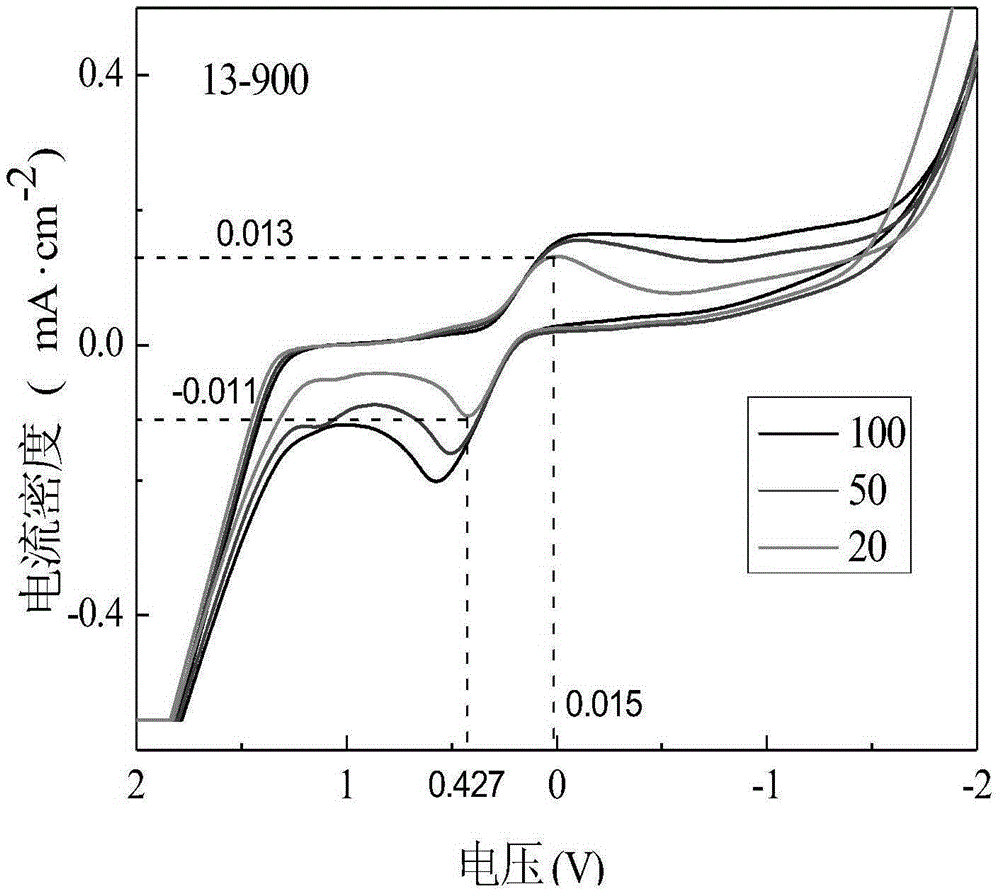
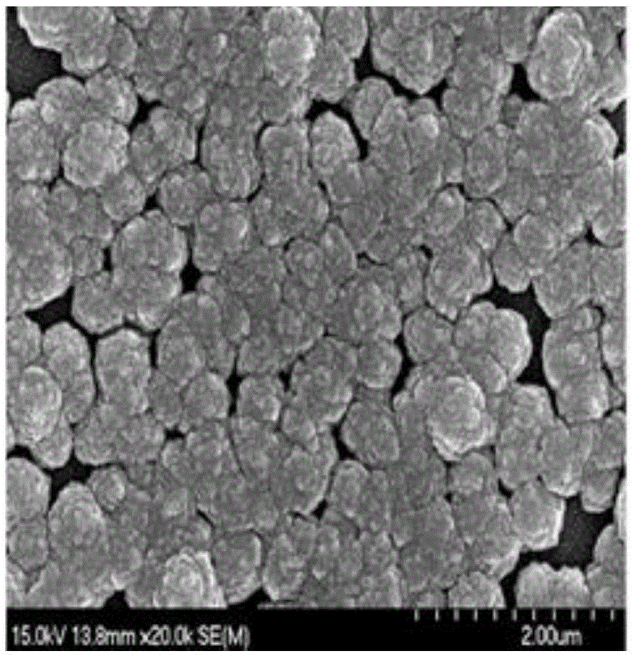
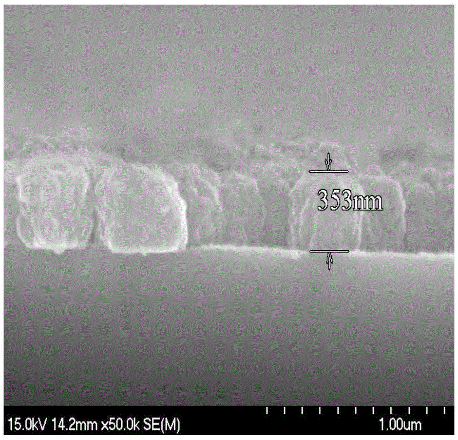
[0039] The monocrystalline silicon wafer is polished with nanometer diamond powder, and the polishing time is about half an hour. Polished silicon wafers were ultrasonically cleaned with deionized water and acetone in turn, dried, and used as substrates for the growth of nano-diamond films. Using hot wire chemical vapor deposition (chemical vapor deposition equipment purchased from Shanghai Jiaoyou Diamond Coating Co., Ltd., model JUHFCVD001), using acetone as the carbon source, acetone was brought into the reaction chamber by hydrogen bubbling, hydrogen, acetone The flow ratio is 200:90, the reaction power is 2000W, the distance between the hot wire and the substrate silicon wafer is 7mm, and the working pressure is 1.63Kpa; no bias is applied during the reaction process, and the preparation time is 15 minutes; The temperature of the sample is cooled under the condition of not flowing hydrogen, and a single particle layer nano-diamond film with a thickness of 300-400nm is pre...

Embodiment 2

[0045] The monocrystalline silicon wafer is polished with nanometer diamond powder, and the polishing time is about half an hour. The polished silicon wafers were washed with deionized water and acetone in an ultrasonic machine, dried, and used as substrates for the growth of nano-diamond films. Using hot wire chemical vapor deposition (chemical vapor deposition equipment purchased from Shanghai Jiaoyou Diamond Coating Co., Ltd., model JUHFCVD001), using acetone as the carbon source, acetone was brought into the reaction chamber by hydrogen bubbling, hydrogen, acetone The flow ratio is 200:90, the reaction power is 2000W, the distance between the hot wire and the substrate silicon wafer is 7mm, the working pressure is 1.63Kpa; no bias is applied during the reaction process, and the film preparation time is 15 minutes. After the growth is completed, the temperature of the sample is cooled under the condition of not flowing hydrogen, and a single particle layer nano-diamond film...

Embodiment 3

[0049] The monocrystalline silicon wafer is polished with nanometer diamond powder, and the polishing time is about half an hour. The polished silicon wafers were washed with deionized water and acetone in an ultrasonic machine, dried, and used as substrates for the growth of nano-diamond films. Using hot wire chemical vapor deposition (chemical vapor deposition equipment purchased from Shanghai Jiaoyou Diamond Coating Co., Ltd., model JUHFCVD001), using acetone as the carbon source, acetone was brought into the reaction chamber by hydrogen bubbling, hydrogen, acetone The flow ratio is 200:90, the reaction power is 2000W, the distance between the hot wire and the substrate silicon wafer is 7mm, the working pressure is 1.63Kpa; no bias is applied during the reaction process, and the film preparation time is 15 minutes. After the growth is completed, the temperature of the sample is cooled under the condition of not flowing hydrogen, and a single particle layer nano-diamond film...


PUM

PropertyMeasurementUnit
thicknessaaaaaaaaaa

Abstract

The invention discloses a preparation method for a boron-doped single-particle-layer nano-diamond film. The method includes the following steps that (1) a hot filament chemical vapor deposition method is adopted for preparing a single-particle-layer nano-diamond film with the thickness being 300-600 nm on a single-crystal silicon substrate; (2) an ion implantation method is adopted, boron ions are injected into the single-particle-layer nano-diamond film obtained in the step (1), and a film with the injected boron ions is obtained; and (3) vacuum annealing is conducted on the film which is obtained in the step (2) and injected with the boron ions, and then the boron-doped single-particle-layer nano-diamond film is obtained. The boron-doped single-particle-layer nano-diamond film prepared through the method has excellent electrochemical performance, especially has good electrochemical catalysis performance, and can be used for electrochemical catalysis oxidation treatment on organic wastewater.

Description

(1) Technical field [0001] The invention relates to a boron-doped single particle layer nanometer diamond film and a preparation method thereof. (2) Background technology [0002] Nano-diamond film has extremely high chemical stability, high temperature and corrosion resistance, good dimensional stability and high hardness, and can be used in electrosynthesis and electrolysis industries. Boron-doped nano-diamond films have excellent electrochemical properties such as wide potential window and low background current. The electrodes prepared by them are very important in the fields of electrolysis, electrosynthesis, electroanalysis, capacitors, and biosensors. scientific significance and engineering value. [0003] The nano-diamond film prepared by chemical vapor deposition (CVD) has staggered and overlapping surface grains, which greatly reduces the specific surface area of ​​the diamond film and reduces its surface activity; boron impurities are doped during the CVD growth ...

Claims


Application Information

Patent Timeline
Patent Type & Authority Applications(China)
IPC IPC(8): C23C16/27C23C14/48C23C14/58C02F1/467C02F101/34
Inventor 胡晓君杭鹏杰俞浩
Owner ZHEJIANG UNIV OF TECH
Why Eureka
Try Eureka