Gallium nitride based high electron mobility transistor epitaxial structure and manufacturing method thereof

A high electron mobility, gallium nitride-based technology, applied in the field of gallium nitride-based high electron mobility transistor epitaxial structure and its manufacturing, can solve the influence of two-dimensional electron gas density and mobility rate, increase buffer layer and gate Leakage current, reducing the RF performance of transistors and other issues, to achieve the effect of improving electron mobility, increasing breakdown voltage, and reducing leakage current

Inactive Publication Date: 2016-02-17
江西省昌大光电科技有限公司
View PDF3 Cites 6 Cited by
  • Summary
  • Abstract
  • Description
  • Claims
  • Application Information

AI Technical Summary

Problems solved by technology

However, due to the lattice mismatch and thermal mismatch between the AlGaN barrier layer and the GaN channel layer, a high density of dislocations will be generated during AlGaN heteroepitaxial growth.
The high density of dislocations in the AlGaN/GaN heterojunction not only increases the leakage current of the buffer layer and the gate

Method used


Image

  • Gallium nitride based high electron mobility transistor epitaxial structure and manufacturing method thereof
  • Gallium nitride based high electron mobility transistor epitaxial structure and manufacturing method thereof
  • Gallium nitride based high electron mobility transistor epitaxial structure and manufacturing method thereof

Examples


Embodiment 1

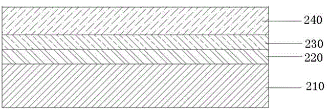
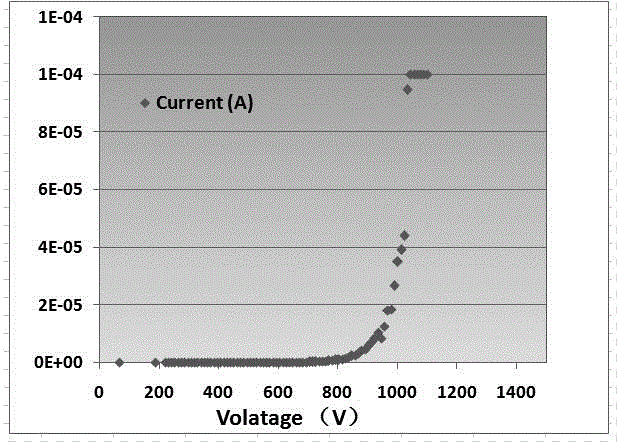
[0023] figure 2 It is a schematic diagram of the epitaxial structure for forming the GaN template layer in the present invention. It grows an AlN nucleation layer 220 , an AlGaN buffer layer 230 , and an Al-doped GaN template layer 240 sequentially on a silicon substrate 210 by MOCVD technology. The specific growth process is as follows: select the silicon (111) substrate 210, and use MOCVD technology to grow; place the silicon (111) substrate 210 in H 2 The surface is treated in the environment for 5 minutes; the temperature is kept constant, and an AlN nucleation layer 220 with a thickness of 0.3um is grown on the silicon substrate 210; an AlGaN buffer layer with a thickness of 0.2um is grown on the AlN nucleation layer 220 230; then add trimethylaluminum to the growth atmosphere to form an Al-doped GaN template layer 240 with a thickness of 2 μm, wherein the concentration of Al doping is 1×10 18 cm -3 ;Turn off gas and cool to room temperature. Then the breakdown volta...

Embodiment 2

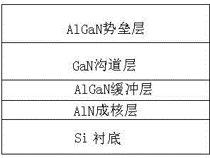
[0025] This embodiment provides a GaN-based high electron mobility transistor, such as Figure 4 As shown, a layer of AlN nucleation layer 320 is grown on a silicon substrate 310, and then an AlGaN buffer layer 330 is grown, and then grown with an aluminum doping concentration of 1×10 16 cm -3 GaN template layer 340, then grow an AlGaN barrier layer 350 and grow a doped or non-doped GaN capping layer 360, and finally make device source, drain ohmic contact electrodes and gate electrodes ( Figure 4 not marked).

Embodiment 3

[0027] This embodiment provides another GaN-based high electron mobility transistor, such as Figure 5 As shown, an AlN nucleation layer 420 is grown on a SiC substrate 410, and then an AlGaN buffer layer 430 is grown, followed by growth of an Al doping concentration of 1×10 16 cm -3 GaN template layer 440, then grow a GaN channel layer 450 with a thickness of 50nm, grow an AlGaN barrier layer 460 and a doped or non-doped GaN cap layer 470 on the channel layer, and finally make the device source, drain ohmic contact electrode and gate electrode ( Figure 5 not marked).


PUM

PropertyMeasurementUnit
Thicknessaaaaaaaaaa

Abstract

The invention discloses a Gallium nitride based high electron mobility transistor epitaxial structure and a manufacturing method thereof. The epitaxial structure comprises a substrate layer on which an AlN nucleating layer, an AlGaN buffer layer, an Al doped GaN template layer and an AlGaN barrier layer grow from bottom to top. Since a method of forming GaN template layer through Al doping is adopted during the process of manufacturing the Gallium nitride based high electron mobility transistor epitaxial structure, the dislocation density of material can be reduced, flatness of a plane can be improved, the electron mobility of the material can be enhanced, the density of states of the surface of heteroepitaxy AlGaN buffer layer can be reduced, the leak current of a device can be lowered further and the breakdown voltage of the device can be improved; in addition, the process is simple and flexible.

Description

technical field [0001] The invention relates to the technical field of semiconductors, in particular to a gallium nitride-based high electron mobility transistor epitaxial structure and a manufacturing method thereof. Background technique [0002] GaN has the characteristics of large direct band gap (3.4ev), high thermal conductivity, and high electron saturation drift velocity, so it has become a research hotspot in the field of semiconductor technology. In particular, GaN-based high electron mobility field-effect transistors (HEMTs) are a new class of electronic devices based on nitride heterostructures. The device has excellent characteristics of high frequency and high power, and is widely used in information transmission and reception, energy conversion and other fields such as wireless communication base stations and power electronic devices. [0003] The principle of High Electron Mobility Transistor (HEMT) is that due to the different bandgap widths of the two mater...

Claims


Application Information

Patent Timeline
IPC IPC(8): H01L29/778H01L29/36H01L21/335
Inventor 陈振王敏周名兵
Owner 江西省昌大光电科技有限公司
Why Eureka
Try Eureka