Method for preparing copper antimony sulfide solar cell light-absorbing layer film
A technology for solar cells and light absorbing layers, which is applied in circuits, electrical components, and final product manufacturing, etc., can solve the problems of poor crystallinity, easy introduction of impurities, low resistance, etc., and achieve the effect of good crystallinity
- Summary
- Abstract
- Description
- Claims
- Application Information
AI Technical Summary
Problems solved by technology
Method used
Image
Examples
Embodiment 1
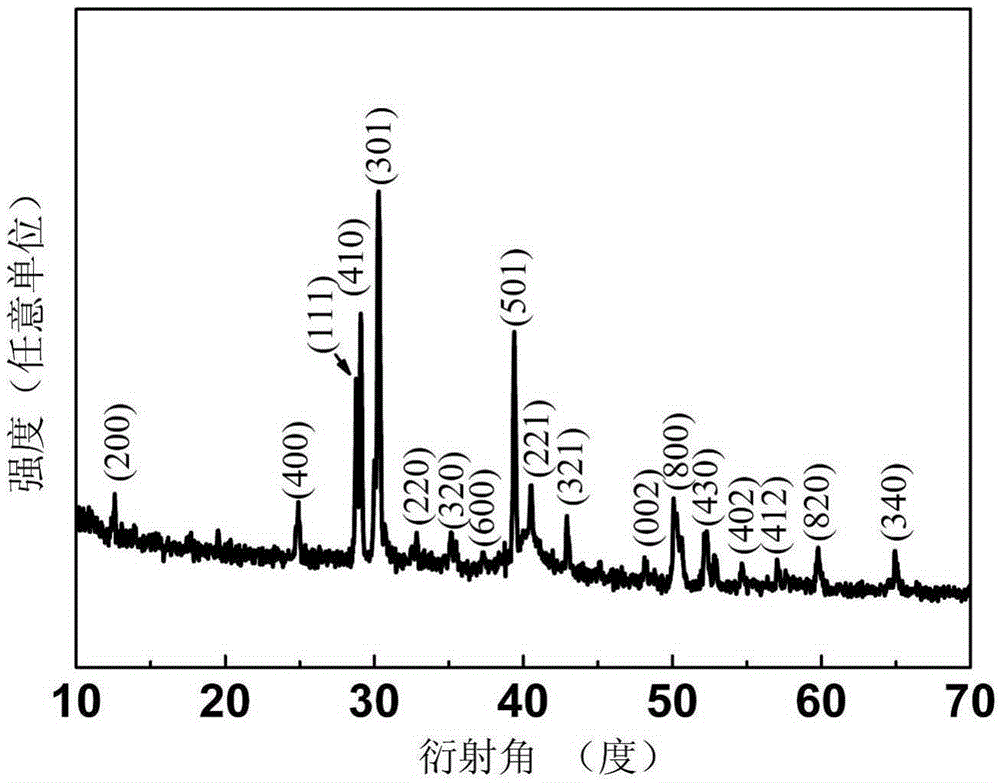
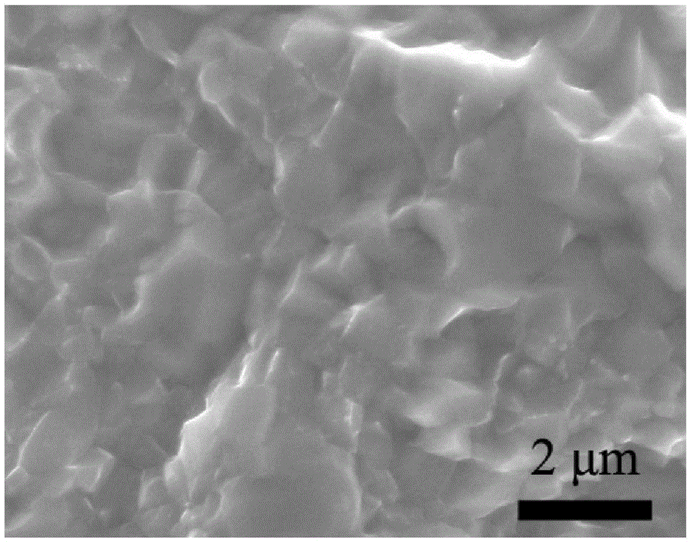
[0022] Embodiment 1: copper antimony sulfur (CuSbS 2 ) film preparation
[0023] 1. Fix the molybdenum-coated glass substrate on the substrate of the multi-source thermal evaporation coating system, close the cavity, and use a mechanical pump and a molecular pump to pump the background vacuum inside the cavity to 5×10 -4 Pa, start the beam source furnace heater, and make sure the beam source furnace damper is closed.
[0024] 2. Raise the temperature of the copper, antimony and sulfur beam source furnaces to 1100-1200°C, 500-600°C and 100-200°C respectively, and keep them constant.
[0025] 3. The substrate heater starts to heat up from room temperature, and rises to 200-300°C in 3-8 minutes and keeps it constant. At this time, open the baffle of the antimony and sulfur beam source furnace to start the first stage of evaporation, and evaporate the molybdenum-coated glass substrate For antimony and sulfur, the first stage of evaporation ends after 10-15 minutes; the second st...
Embodiment 2
[0027] With copper antimony sulfur (CuSbS) of the present invention 2 ) film to prepare solar cells, the structure of which is as image 3 As shown, the specific process of the preparation method is as follows:
[0028] 1. Plating a molybdenum back electrode layer with a thickness of 600 nanometers on the soda-lime glass by DC magnetron sputtering;
[0029] 2. Preparation of 1.2 μm thick copper antimony sulfur (CuSbS) on molybdenum-coated glass by three-step co-evaporation 2 ) thin film light absorbing layer;
[0030] 3. Prepare a cadmium sulfide buffer layer with a thickness of 50 nanometers by chemical bath method;
[0031] 4. Prepare a 100 nm thick intrinsic zinc oxide layer by magnetron sputtering;
[0032] 5. Prepare a 500-nanometer thick indium tin oxide transparent conductive window layer by magnetron sputtering;
[0033] 6. Preparation of silver electrodes by thermal evaporation.
[0034] The SEM photo of the section of the copper antimony sulfur thin film solar ce...
PUM
 Abstract
Description
Claims
Application Information


