Method for regulating and controlling threshold voltage of semiconductor nanowire field effect transistor

A field-effect transistor and threshold voltage technology, applied in semiconductor devices, semiconductor/solid-state device manufacturing, circuits, etc., can solve the problem of reducing the carrier density in nanowires, and achieve easy large-scale industrial production, reliable principle, and operation easy effect

Inactive Publication Date: 2016-06-01
QINGDAO UNIV
View PDF1 Cites 9 Cited by
  • Summary
  • Abstract
  • Description
  • Claims
  • Application Information

AI Technical Summary

Problems solved by technology

[0003] In order to control the working mode of NWFET, several different processes have been developed to control the threshold voltage of NWFET, for example, by controlling the surface morphology of ZnO nanowires to generate different surface electron trap densities, thereby regulating the free carrier density. Density, and finally enhanced and depleted FETs can be obtained (W.K.Hong, J.I.Sohn, D.K.Hwang, et al., TunableElectronicTransportCharacteristicsofSurface-Architecture-ControlledZnONanowireFieldEffectTransistors, NanoLett., 8, 950, (2008)); Liao et al. use metal doping In 2 o 3 Nanowires to compensate the oxygen vacancies in the nanowires, thereby reducing the carrier density in the nanowires, so that the threshold voltage of the NWFET moves toward the positive voltage direction, and finally an enhanced NWFET is obtained (X.M.Zou, J.L.Wang, X.Q.Liu, et al. ,ControllableElectricalPropertiesofMetal-DopedIn 2 o 3 Nanowires for High-PerformanceEnhancementModeTransistors, NanoLett., 13, 3287 (2013)); Tomioka et al. successfully regulated the threshold voltage of the device by using a metal-wrapped vertical structure InGaAs NWFET gate with a higher work function (K.Tomioka, M.Yoshimura , T.Fukui, AIII–VNanowireChannelonSiliconforHigh-PerformanceVerticalTransistors,Nature,488,189(2012)), however, the complex gate structure will limit the application of this element in electronic devices, sensors and other fields; Han et al. use metal nanowires with different work functions Particles modify the surface of InAs, InP, and InGaAs nanowires, successfully realize the threshold voltage regulation of III-V nanowires, obtain depletion-type and enhancement-type NWFETs, and assemble them together to obtain efficient n-type reverse Device (N.Han, F.Y.Wang, J.J.Hou, etal., TunableElectronicTransportPropertiesofMetal-ClusterDecoratedIII–VNanowireTransistors, Adv.Mater., 25, 4445 (2013)); but metal nanoparticles are unstable in the air and need to be on the surface of the nanowire Deposit a layer of 20nm Al 2 o 3 protective layer, however Al 2 o 3 Layers will limit the application of such devices in the fields of sensors, detectors, etc.; recently, Cheung et al. have used aromatic thiolate monolayers to modify the surface of InAs nanowires. This monolayer can not only passivate the surface states of InAs nanowires and thus Improve its electron mobility, and the aromatic thiolate with electron-donating and electron-withdrawing groups can also adjust the threshold voltage of InAsNWFET to move to positive and negative voltages respectively (H.Y.Cheung, S.P.Yip, N.Han, et al., Modulating Electrical Properties of InAs Nanowires via Molecular Monolayers, ACSNano, 9, 7545 (2015)); However, the aromatic thiolate monolayer has limited ability to attract free electrons in InAs nanowires, and can only move the threshold voltage of InAs NWFETs to the positive direction by 1.5V, which is difficult to enhance type FET; in addition, because the aromatic thiolate cannot exist stably in the air for a long time, the threshold voltage of the device modified by the molecular layer cannot remain unchanged in the air for a long time

Method used


Image

  • Method for regulating and controlling threshold voltage of semiconductor nanowire field effect transistor
  • Method for regulating and controlling threshold voltage of semiconductor nanowire field effect transistor
  • Method for regulating and controlling threshold voltage of semiconductor nanowire field effect transistor

Examples


Embodiment 1

[0036] The specific process steps for regulating the threshold voltage of the semiconductor NWFET in this embodiment are:

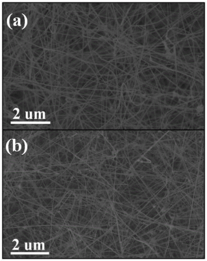
[0037] (1) First, disperse the prepared InAs nanowires in absolute ethanol, and ultrasonically disperse them evenly;

[0038] (2) Disperse one-dimensional semiconductor nanomaterials on the surface to cover 50nm SiO by low drop coating method 2 On the p-type heavily doped silicon wafer of the dielectric layer;

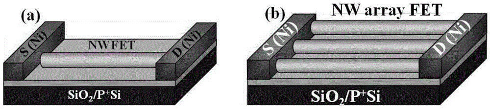
[0039] (3) Prepare photoresist patterns of source and drain electrodes on the p-type heavily doped silicon wafer obtained in step (2) by photolithography, evaporate and deposit 80nmNi film as source and drain electrodes by thermal evaporation, and then lift off the metal by metal stripping The process removes unnecessary photoresist and metal film, and completes the preparation of the back gate InAsNWFET;

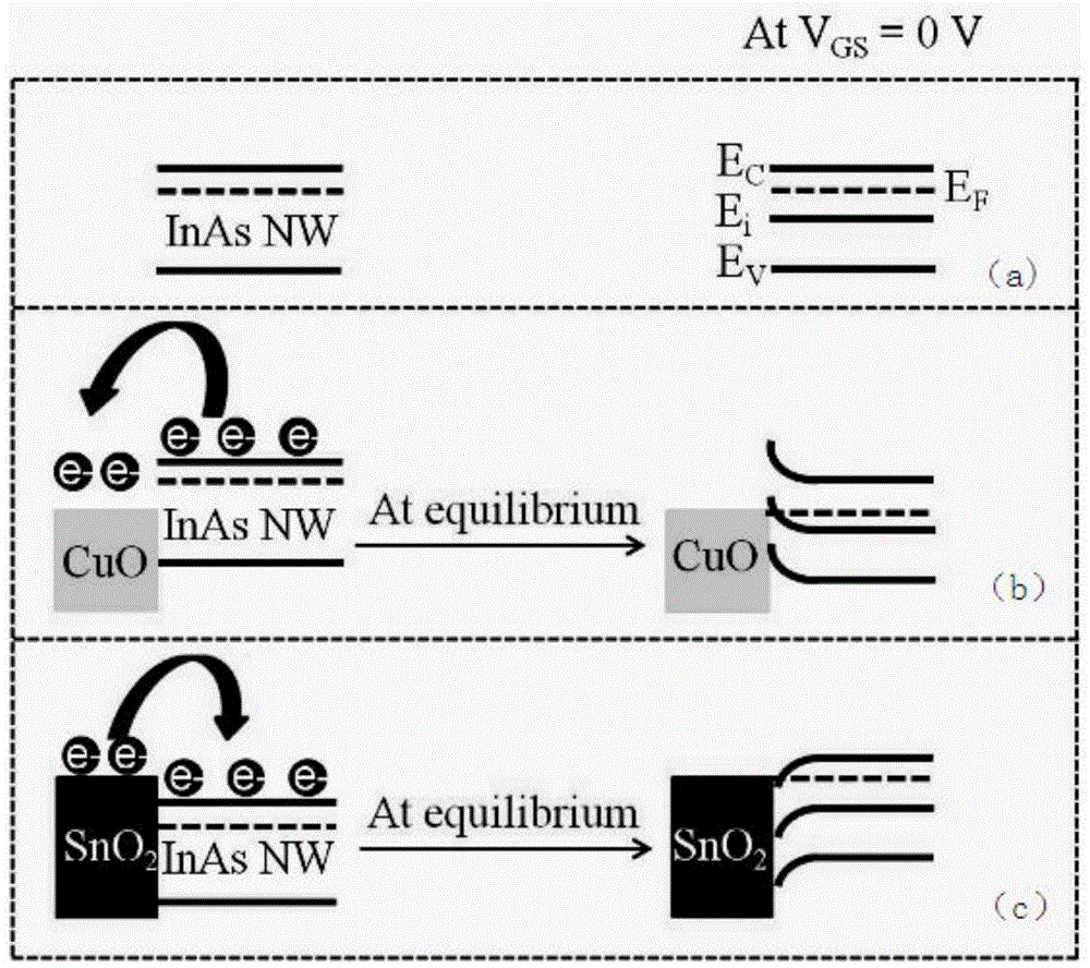
[0040] (4) A 0.5nm Cu film was evaporated on the prepared back-gate InAsNWFET by thermal evaporation, and then annealed at a low temperature...

Embodiment 2

[0042] In the present embodiment, the deposition thickness of the Cu film is 0.2nm, and other experimental conditions are the same as in Example 1. The experiment shows that the CuO nanoparticles formed by the 0.2nm thick Cu film can move the threshold voltage of a single InAsNWFET towards the positive voltage direction, Figure 6 a is the transfer curve of a single InAsNWFET before and after modification with CuO nanoparticles formed by a 0.2nm thick Cu film, indicating that the CuO nanoparticles formed by a 0.2nm Cu film can successfully transform the threshold value of a single nanowire diameter ~ 30nm InAsNWFET The voltage moves ~2.1V to the positive voltage direction; the threshold voltage of the modified NWFET is ~0V, becoming an enhanced InAs NWFET.

Embodiment 3

[0044] In this embodiment, the deposition thickness of the Cu thin film is 2.0nm to modify the surface of the InAs nanowires. Other experimental conditions are the same as in Example 1. The experiment shows that the CuO nanoparticles formed by the 2.0nm Cu thin film can convert a single InAs NWFET from the depletion mode transformed into enhanced, Figure 6 b is the transfer curve of a single InAs NWFET before and after modification with CuO nanoparticles formed by a 2.0nm Cu film, indicating that the CuO nanoparticles formed by a 2.0nm Cu film can change the threshold voltage of an InAs NWFET with a single nanowire diameter ~ 30nm to a positive voltage The direction shifted to ~6.2V; the threshold voltage of the modified InAsNWFET was ~5.0V, successfully transformed into an enhancement mode.


PUM


Abstract

The invention belongs to the field of transistor threshold voltage regulating and controlling technology, and relates to a method for regulating and controlling threshold voltage of a semiconductor nanowire field effect transistor. The method comprises steps of depositing metal-oxide semiconductor materials or metal materials on a prepared semiconductor nanowire field effect transistor or a prepared nanowire array field effect transistor, and carrying out film coating decoration on the surface of the semiconductor nanowire field effect transistor or on the surface of the nanowire array field effect transistor, wherein thickness of a coating film is 0.2-5 nm, thereby regulating and controlling the threshold voltage of the semiconductor nanowire field effect transistor or the nanowire array field effect transistor. According to the invention, the technique is simple; operation is simple; principles are reliable; product cost is low; the method has a wide application prospect in field of electronic switch devices, displays, and biological and chemical sensors; and large-scale industrial production can be easily carried out.

Description

Technical field: [0001] The invention belongs to the technical field of transistor threshold voltage regulation, and relates to a method for regulating the threshold voltage of a semiconductor nanowire field-effect transistor (NWFET), in particular to a method for regulating III-V and metal oxide semiconductor NWFETs by using metal oxide semiconductor nanoparticles The threshold voltage technology can be widely used in high-performance sensors, detectors, optoelectronic devices and other fields. Background technique: [0002] With the development of nanotechnology, one-dimensional semiconductor nanomaterials have become a research hotspot. Compared with bulk materials, semiconductor nanowires have many advantages. For example, due to their small size, nanowires can not only greatly save material costs, improve material utilization efficiency, but also effectively increase the assembly density of devices; Axial and axial p-n, p-i-n heterojunction can improve the conversion e...

Claims


Application Information

Patent Timeline
Patent Type & Authority Applications(China)
IPC IPC(8): H01L21/336H01L29/775
CPCH01L29/66439H01L29/775
Inventor 王凤云韩宁
Owner QINGDAO UNIV
Why Eureka
Try Eureka