Rapid preparation method for cuprous oxide nano-film

A nano-film, cuprous oxide technology, applied in the field of rapid preparation of cuprous oxide nano-film, can solve the problems of poor quality of cuprous oxide film, long preparation period, high energy consumption, etc., achieve obvious absorption, accurate and detailed data, Combines a strong effect

Inactive Publication Date: 2016-06-22
TAIYUAN UNIV OF TECH
View PDF3 Cites 12 Cited by
  • Summary
  • Abstract
  • Description
  • Claims
  • Application Information

AI Technical Summary

Problems solved by technology

[0002] Cuprous oxide is a p-type semiconductor material with a bandgap between 2-2.2eV. Due to its high light absorption coefficient, abundant resources and non-toxicity, it is widely used in solar energy conversion, microelectronics, catalysis and other fields; especially Cuprous oxide thin films have been widely used in moisture sensors, electrochromic devices and photovoltaic devices; cuprous oxide thin films are usually prepared by magnetron sputtering, pulsed laser beam deposition, chemical vapor deposition, thermal oxidation and hydrothermal synthesis methods; However, magnetron sputtering, pulsed laser beam deposition, chemical vapor deposition, and thermal oxidation require expensive equipment and consume a lot of energy; while the cuprous oxide films prepared by hydrothermal synthesis are of poor quality and have a long preparation cycle

Method used


Image

  • Rapid preparation method for cuprous oxide nano-film
  • Rapid preparation method for cuprous oxide nano-film
  • Rapid preparation method for cuprous oxide nano-film

Examples


Embodiment Construction

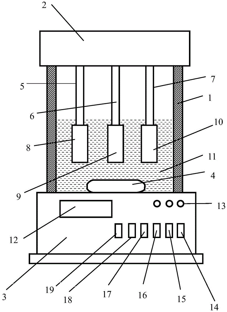
[0083] The present invention will be further described below in conjunction with accompanying drawing:

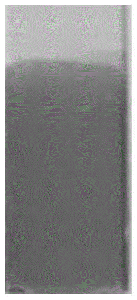
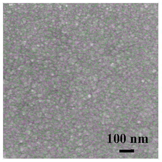
[0084] figure 1 As shown, in order to prepare the state diagram of the cuprous oxide nano film, the position and connection relationship of each part must be correct, the ratio should be proportioned, and the operations should be performed in sequence.

[0085] Quantities of the chemical substances used in the preparation are determined according to a preset range, with grams, milliliters, and millimeters as measurement units.

[0086] The preparation of cuprous oxide nano film is carried out in a glass electrolytic cell, in an alkaline copper acetate electrolyte, with conductive glass as a working electrode, a platinum sheet as a counter electrode, and a silver chloride sheet as a reference electrode. At ℃, in the process of magneton stirring, under the DC pulse current, the cuprous oxide nano film is deposited on the conductive glass;

[0087] The glass electrolytic cel...


PUM

PropertyMeasurementUnit
thicknessaaaaaaaaaa
diameteraaaaaaaaaa

Abstract

The invention relates to a rapid preparation method for a cuprous oxide nano-film. According to the structural features of cuprous oxide, copper acetate and lactic acid are adopted as raw materials, lauryl sodium sulfate is used as a surface dressing agent, deionized water is used as a solvent, sodium hydroxide is adopted as a pH alkaline modifier, and the cuprous oxide nano-film is prepared through an electrochemical pulse direct-current electrolytic method. According to the rapid preparation method, the process is advanced, data are accurate and full, the nano-film is a yellow film, the section of the nano-film is rectangular, and the film thickness is smaller than or equal to 30 nm; the cuprous oxide nano-film is composed of particles which are in the shape of nano-balls, the diameter of the particles is smaller than or equal to 30 nm, and product purity reaches 99.6%; combination between the nano-film and conductive glass is firm, the nano-film can obviously absorb ultraviolet light and visible light, currents of 240 [mu]A / cm2 can be generated under irradiation of a 100W xenon lamp, and the nano-film can be used for solar power generation and photovoltaic products; the rapid preparation method for the cuprous oxide nano-film is advanced.

Description

technical field [0001] The invention relates to a rapid preparation method of cuprous oxide nano film, which belongs to the technical field of preparation and application of inorganic functional materials. Background technique [0002] Cuprous oxide is a p-type semiconductor material with a bandgap between 2-2.2eV. Due to its high light absorption coefficient, abundant resources and non-toxicity, it is widely used in solar energy conversion, microelectronics, catalysis and other fields; especially Cuprous oxide thin films have been widely used in moisture sensors, electrochromic devices and photovoltaic devices; cuprous oxide thin films are usually prepared by magnetron sputtering, pulsed laser beam deposition, chemical vapor deposition, thermal oxidation and hydrothermal synthesis methods; However, magnetron sputtering, pulsed laser beam deposition, chemical vapor deposition, and thermal oxidation require expensive equipment and consume a lot of energy; while the cuprous ox...

Claims


Application Information

Patent Timeline
Patent Type & Authority Applications(China)
IPC IPC(8): C25D9/04B82Y40/00
CPCC25D9/04B82Y40/00
Inventor 薛晋波申倩倩杨慧娟邵铭哲胡文岳贾虎生许并社
Owner TAIYUAN UNIV OF TECH
Why Eureka
Try Eureka