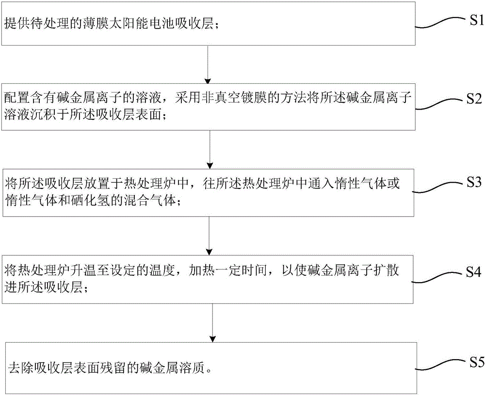
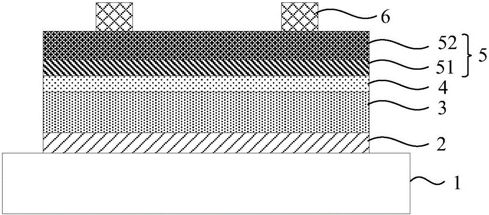
Alkali metal doping method for thin-film solar cell absorption layer
A technology of solar cells and absorption layers, applied in the field of solar cells, can solve the problems of low material utilization rate and high cost of thin film deposition equipment, and achieve the effects of good compatibility, simple and controllable preparation method, and high utilization rate
- Summary
- Abstract
- Description
- Claims
- Application Information
AI Technical Summary
Problems solved by technology
Method used
Image
Examples
Embodiment 1
[0058] Step 1. Soda-lime glass is used as the substrate, ultrasonically cleaned, then dried with pure nitrogen and placed in a magnetron sputtering vacuum chamber, dehydrated and degassed, and a double-layer Mo back electrode layer is deposited by DC magnetron sputtering, with a thickness of 0.6μm;
[0059] Step 2, put the substrate prepared with the Mo back electrode layer into the vacuum chamber, and wait for the vacuum degree to be better than 1×10 -3 After Pa, use CuGa alloy target (Ga content at.25%) and In target to co-sputter deposit CuInGa (CIG) metal prefabricated layer with a thickness of 0.6 μm;
[0060] Step 3, transfer the substrate prepared with the metal prefabricated layer into the selenization furnace, and use H 2 Se was used as a selenium source, selenized at 400°C for 30 minutes, annealed in a nitrogen atmosphere at 580°C for 30 minutes, and then cooled naturally to prepare a CIGS absorbing layer with a thickness of 1.2 μm;
[0061] Step 4. Use potassium f...
Embodiment 2
[0069] Step 1. Soda-lime glass is ultrasonically cleaned, then dried with pure nitrogen and placed in a magnetron sputtering vacuum chamber, dehydrated and degassed, and a double-layer Mo back electrode layer is deposited by DC magnetron sputtering, with a thickness of 0.6 μm;
[0070] Step 2, put the substrate prepared with the Mo back electrode layer into the vacuum chamber, and wait for the vacuum degree to be better than 1×10 -3 After Pa, use CuGa alloy target (Ga content at.25%) and In target to co-sputter deposit CuInGa (CIG) metal prefabricated layer with a thickness of 0.6 μm;
[0071] Step 3, transfer the substrate prepared with the metal prefabricated layer into the selenization furnace, and use H 2 Se was used as a selenium source, selenized at 400°C for 30 minutes, annealed in a nitrogen atmosphere at 580°C for 30 minutes, and then cooled naturally to prepare a CIGS absorbing layer with a thickness of 1.2 μm;
[0072] Step 4: Use KF powder and dimethyl sulfoxide (...
Embodiment 3
[0080] Step 1. Soda-lime glass is ultrasonically cleaned, then dried with pure nitrogen and placed in a magnetron sputtering vacuum chamber, dehydrated and degassed, and a double-layer Mo back electrode layer is deposited by DC magnetron sputtering, with a thickness of 0.6 μm;
[0081] Step 2, put the substrate prepared with the Mo back electrode layer into the vacuum chamber, and wait for the vacuum degree to be better than 1×10 -3 After Pa, the CIGS absorbing layer was prepared by co-evaporation method with a thickness of 2 μm;
[0082] Step 3. Use potassium fluoride (KF) powder and deionized water to configure a 0.5mol / L KF aqueous solution, and use a spin coating device to evenly spin coat the KF aqueous solution on the surface of the CIGS absorbing layer at a spin coating speed of 4000r / min. Coating time is 3min, spin coating once, spin coating process H 2 O evaporates and forms a KF film on the CIGS surface;
[0083] Step 4, place the CIGS absorbing layer with the KF t...
PUM
| Property | Measurement | Unit |
|---|---|---|
| Thickness | aaaaa | aaaaa |
Abstract
Description
Claims
Application Information


