A Holographic Imaging Film Based on Surface Plasmon Coupling Structure

A surface plasmon and coupling structure technology, applied in nanotechnology, instruments, etc., can solve problems such as limited development, image distortion, and difficult adjustment of hologram color, and achieve the effect of improving reflection efficiency and wide viewing angle

Active Publication Date: 2019-01-11
PEKING UNIV
View PDF7 Cites 0 Cited by
  • Summary
  • Abstract
  • Description
  • Claims
  • Application Information

AI Technical Summary

Problems solved by technology

The main reason is that the traditional holographic technology relies on special photosensitive materials for photoresists, which is essentially a non-real-time optical processing technology, and the operation steps are cumbersome and complicated, which limits its further development.
On the other hand, because the color of the hologram is difficult to adjust, the imaging depends on the photosensitive material, and the optical annihilation and readout error of the material itself will easily cause a certain degree of image distortion, and the image data reading process is cumbersome, and it is difficult to perform real-time imaging. It hinders the further development and marketization of 3D display holographic technology

Method used


Image

  • A Holographic Imaging Film Based on Surface Plasmon Coupling Structure
  • A Holographic Imaging Film Based on Surface Plasmon Coupling Structure
  • A Holographic Imaging Film Based on Surface Plasmon Coupling Structure

Examples


Embodiment 1

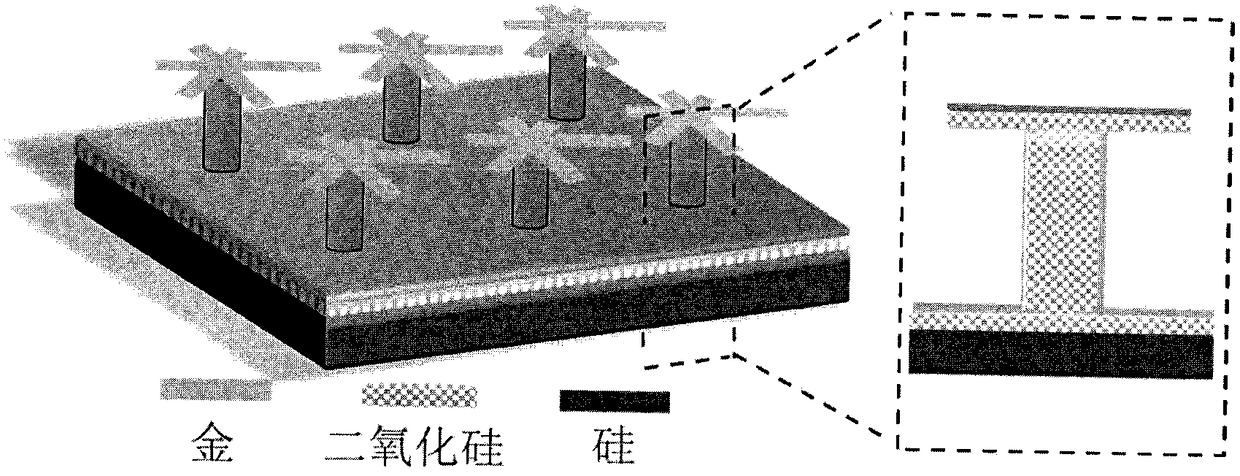
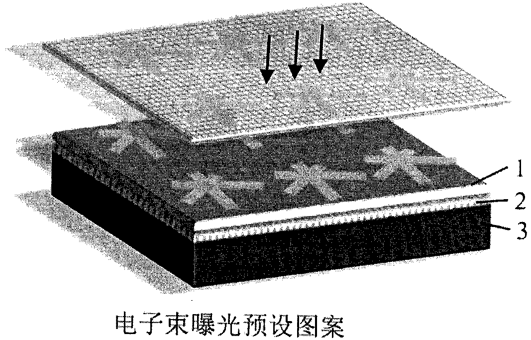
[0022] (1) thermal oxidation passivation layer: utilize thermal oxidation growth on the surface of silicon (Si) substrate 1 Thick SiO 2 as a passivation layer.

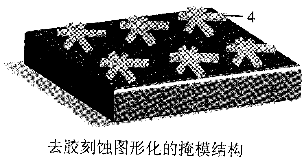
[0023] (2) Photolithographic patterning: Take AR-N7520.18 negative photoresist as an example, spin-coat it with a thickness of 100nm at a speed of 5000 rpm, and pre-bake it in an oven at 85°C for 5 minutes, using NanoBeam electronics The beam etching system exposes the photoresist with an accelerating voltage of 80kV, develops it in tetramethylammonium hydroxide (TMAH) developer solution for 1 minute, and rinses it with deionized water to obtain an imaged nanostructure array;

[0024] (3) Formation of insulating dielectric nanocolumns: use silicon oxide as a mask, etch the silicon substrate with a reactive ion etching machine, the power of the etching machine is 400W, SF 6 and C 4 f 8 The flow rates were 40 and 90 sccm / min, the etching time was 50 seconds, and SF 6 As an etching gas, C 4 f 6 As the polymer gen...


PUM


Abstract

The invention discloses a holographic imaging film based on a surface plasma coupling structure. Electron beam lithography is used to prepare an asymmetric nanostructure layer. According to the nano processing technology, Bosch technology is used for reactive ion etching, SF6 is used for etching, C4F6 is used to generate a polymer, etching and passivation are carried out alternatively, the scallop-shaped sidewall shape is formed via horizontal undercutting, a dielectric nano column is obtained, a metal film is deposed in the direction vertical to a substrate, and a metal nanostructure-metal film coupling structure is obtained. A meta-material of the sub-wavelength coupling structure presents harmonic resonance and dark-field excitation plasma resonance modes in a visible light spectrum, multi-formant narrowband resonance is generated, the asymmetric upper-layer nanostructure enables that a reflection array is flexible in color response and high in reflectivity to different incident fields, the reflection array can be applied to the holographic imaging film of color holographic imaging, real 3D images of objects can be recorded and reproduced in real time, and the imaging film can realize real space imaging, is brilliant in colors and high in contrast and sharpness, and can be applied to the fields including commodity display, video production and creation.

Description

technical field [0001] The present invention relates to nanofabrication and manufacturing technology, surface plasmon photonics, and physical optics imaging technology, in particular to a reflective array metamaterial based on surface plasmon coupling resonance effect, and its unique application in full true-color holographic imaging technology. Background technique [0002] Three-dimensional (3D) display technology is divided into two types: one is to use the parallax characteristics of the human eye to produce a three-dimensional effect; the other is to display real 3D stereoscopic images in space, such as stereoscopic imaging based on holographic imaging technology. The hologram uses laser as the light source, using two coherent laser beams. First, the laser beam 1 irradiates the object in the dark room. At the same time, the object emits a scattered laser wave to the space, which is called the object reflected laser wave. In addition, the laser beam 2 emits a laser wave t...

Claims


Application Information

Patent Timeline
Patent Type & Authority Patents(China)
IPC IPC(8): G03H1/00B82Y40/00
CPCB82Y40/00G03H1/0005
Inventor 吴文刚樊姣荣朱佳
Owner PEKING UNIV
Why Eureka
Try Eureka