Solution preparing method for CsPbI3 film and application of photovoltaic device thereof
A thin-film and solution technology, applied in the materials of organic semiconductor devices, semiconductor/solid-state device fabrication, fabrication/processing of organic semiconductor devices, etc. To avoid problems such as chemical chemistry, to achieve the effect of simple preparation method, avoiding expensive vacuum evaporation equipment investment, and avoiding cumbersome glove box operation
- Summary
- Abstract
- Description
- Claims
- Application Information
AI Technical Summary
Problems solved by technology
Method used
Image
Examples
Embodiment 1
[0032] In this example, CsPbI 3 The film solution preparation method includes the following steps:
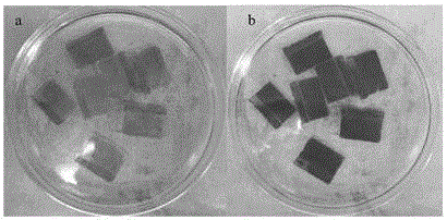
[0033] 1. CsPbI 3 Preparation of precursor solution: mix 0.5mmol CsI (129mg) and 0.5mmol PbI 2 (231mg) was added to 2mL DMF (N,N-dimethylamide) and stirred until the dissolution was complete, and then 66μL HI (57wt%) was added to aid the dissolution, and the stirring was continued until the dissolution was complete, and left to stand for 48hrs to obtain yellow CsPbI 3 Precursor solution, such as figure 2 (a) shown;
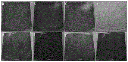
[0034] 2. CsPbI 3 Preparation of precursor film: spin-coating the CsPbI on FTO glass substrate 3 The precursor solution, the rotation speed is 2000rpm, the spin coating time is 30s, and then it is placed on a hotplate at 100℃ and dried for 10min to obtain CsPbI 3 Precursor film, such as figure 2 As shown in (b), while the film is placed in the air, the phase change occurs rapidly, such as image 3 (a) shown;
[0035] 3. CsPbI 3 Preparation of the film: Add 30 mL of isopr...
Embodiment 2
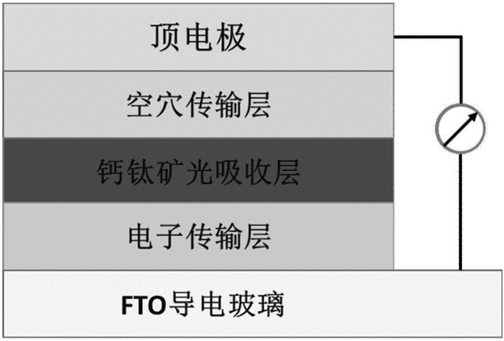
[0037] In this example, CsPbI 3 The structure diagram of the inorganic perovskite photovoltaic device is as figure 1 As shown, the FTO conductive glass is used as the substrate, and the electron transport layer and CsPbI are sequentially deposited on the surface where the FTO film of the FTO conductive glass is located from bottom to top. 3 The light absorbing layer film, the hole transport layer and the top electrode, the specific preparation methods are:
[0038] 1. Deposit a dense layer of TiO on the surface of the FTO film of FTO conductive glass 2 The thin film serves as the electron transport layer: that is, a dense layer of TiO is deposited on FTO glass (purchased directly) by spin-coating isopropyl titanate ethanol solution 2 , And then sintered in air at 450~500℃ for 30~60min to obtain dense layer of TiO 2 Thin film; the dense layer TiO 2 Film immersed in 40mM TiCl 4 In an aqueous solution, treat at 70°C for 30 minutes, and then sinter at 450 to 500°C for 30-60 minutes to o...
Embodiment 3
[0046] In this example, the perovskite solar cell was prepared in the same manner as in Example 2, except that the standing aging time in step 2 was 6 hrs.
PUM
 Abstract
Description
Claims
Application Information


