Forming method of coating film and manufacturing method of light emitting diode device

A coating and coating technology, applied in the direction of electric solid device, semiconductor device, electric light source, etc., can solve the problems of uneven activation of spray coating forming material, poor appearance of dirt, poor electrical contact, etc., and achieve wire bonding. Excellent properties, excellent oxidation resistance, and ease of use

Inactive Publication Date: 2019-11-29
SUMITOMO METAL MINING CO LTD
View PDF11 Cites 0 Cited by
  • Summary
  • Abstract
  • Description
  • Claims
  • Application Information

AI Technical Summary

Problems solved by technology

However, there are the following problems: silver is easy to change color in the air, especially in the environment containing sulfur, it is corroded, and the color becomes dark brown or blue-black, and the electrical contact becomes poor.
However, the thickness of the coating layer formed by this technique is about 300nm, so applying this technique to the coating film of the reflective part of the LED device has problems in terms of wire bonding characteristics
In addition, in this technique, since the plasmaization of the gas and the activation of the atomized spray coating forming material are performed at the same time, the activation of the spray coating forming material becomes uneven, and it is difficult to cover the entire surface of the substrate without omission. form a dense coating
In particular, when there is a passivation film on the surface of the metal material to be coated, or when a noble metal is used as the metal material, the above-mentioned surface state is inactive and in a low-energy state, so the coating film composed of organic substances is formed without omission. is extremely difficult
Therefore, even if an extremely thin coating film can be formed on the surface of a metal coating such as silver by this technology, there may be problems in appearance such as uneven treatment and dirt caused by the surface.

Method used


Image

  • Forming method of coating film and manufacturing method of light emitting diode device
  • Forming method of coating film and manufacturing method of light emitting diode device
  • Forming method of coating film and manufacturing method of light emitting diode device

Examples


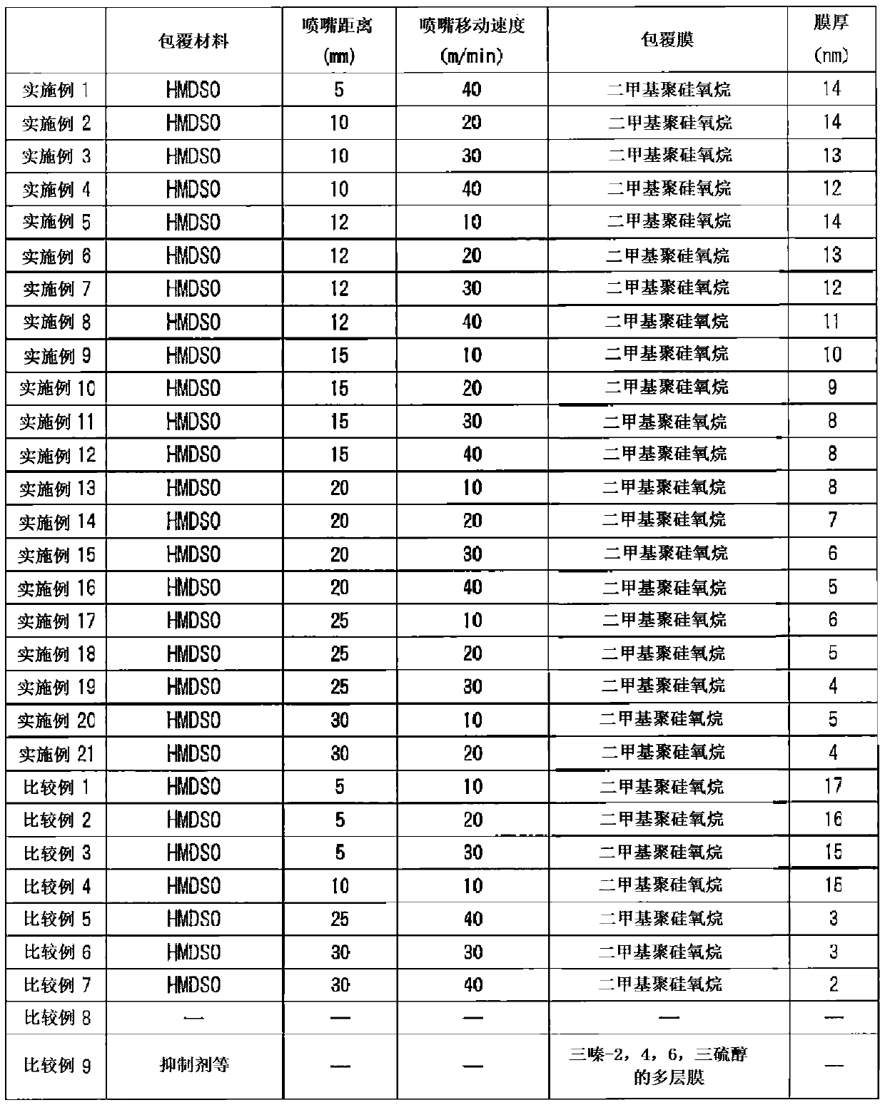
Embodiment 1~21、 comparative example 1~7

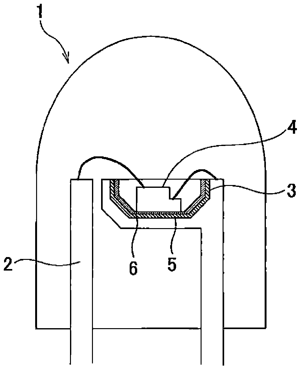
[0089] In Examples 1 to 21 and Comparative Examples 1 to 7, samples obtained by performing silver plating (brightness L value: 70) with a thickness of 4 μm on a pure copper substrate by an electrolytic plating method were used. The base material is formed into a coating film treated with the atmospheric pressure plasma polymerization of the present invention. The conditions of the atmospheric pressure plasma polymerization treatment at this time are as follows.

[0090] (Conditions for Atmospheric Pressure Plasma Polymerization Treatment)

[0091] The transmission frequency of the plasma generator: 21kHz

[0092] Generator output voltage: 280V

[0093] Pressure: atmospheric pressure (1013.25hPa)

[0094] Import amount of hexamethyldisiloxane: 20g / h

[0095] Carrier gas and plasma gas: nitrogen (nitrogen content: 100%)

[0096] In addition, in Examples 1 to 21 and Comparative Examples 1 to 7, the nozzle distance and the nozzle moving speed at the time of forming the coatin...

Embodiment 22、23

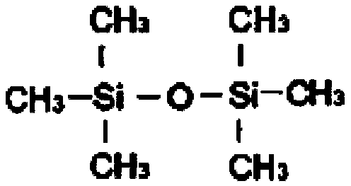
[0113] In Example 22, a sample obtained in the same manner as in Example 1 was used except that decamethyltetrasiloxane (DMTSO) was used as the material of the coating film. In addition, in Example 23, a sample obtained in the same manner as in Example 1 was used except that octamethylcyclotetrasiloxane (OMCTSO) was used as the material of the coating film.

[0114] The coating films formed on the surfaces of these samples were analyzed using an infrared spectroscopic analyzer. As a result, it was confirmed that these coating films were all composed of the structural formula: (CH 3 ) 3 SiO-[(CH 3 ) 2 SiO] n -Si (CH 3 ) 3 Indicates the composition of dimethylpolysiloxane. Moreover, as a result of evaluating the said sample (a)-(c), it was confirmed that it has the same characteristic as Examples 1-21.

Embodiment 24

[0116] A sample obtained in the same manner as in Example 1 was used except that a material in which a part of the side chain of hexamethyldisiloxane (HMDSO) was substituted with a carboxyl group was used as the material of the coating film.

[0117] The coating film formed on the surface of the sample was analyzed using an infrared lead spectrometer, and as a result, it was confirmed that the coating film was composed of the structural formula: (CH 3 ) 3 SiO-[(CH 3 ) 2 SiO] m -[(C 6 h 5 ) 2 SiO] n -Si(CH 3 ) 3 Represents the composition of methylphenyl polysiloxane. Moreover, as a result of evaluating the above-mentioned (a)-(c) about this sample, it was confirmed that it has the characteristic equivalent to Examples 1-21.


PUM

PropertyMeasurementUnit
thicknessaaaaaaaaaa
thicknessaaaaaaaaaa
thicknessaaaaaaaaaa

Abstract

The subject of the present invention is to form a coating film on the surface of a metal material that can prevent discoloration due to corrosion on the surface of the metal material even when it is used during heat treatment at the time of manufacture or in an outdoor environment for a long time , and excellent wire bonding characteristics. The solution of the present invention is to make the hexamethyldisiloxane compound free radical by mixing and spraying the hexamethyldisiloxane compound with nitrogen as a carrier gas in nitrogen plasma gas under atmospheric pressure conditions. , so as to polymerize, and form a polysiloxane film with a thickness of 4nm to 14nm on the surface of the metal material. The polysiloxane film has a main chain of -(Si-O-Si) n ‑ Made of polysiloxane.

Description

technical field [0001] The present invention relates to a coating film formed on the surface of a metal material, especially silver or silver alloy, a method for forming the coating film, and a light emitting diode device provided with the coating film. Background technique [0002] Connectors and lead frames, which are connecting parts for electronic equipment, are often used in which copper and nickel base plating is applied to the surface of copper alloy materials such as brass and phosphor bronze, and silver plating is performed thereon. Since silver is a good conductor of electricity and heat, it is widely used as a plating material for connectors and lead frames. However, there is a problem that silver is easily discolored in the air, and especially corroded in an environment containing sulfur, discoloration becomes dark brown or blue-black, and electrical contact deteriorates. [0003] In recent years, from the viewpoint of energy saving and environmental protection,...

Claims


Application Information

Patent Timeline
Patent Type & Authority Patents(China)
IPC IPC(8): C23C26/00B05D7/24F21S2/00H01L33/62
CPCB05D1/62B05D5/08C09D183/04H01L33/44H01L33/60H01L2224/45144H01L2224/48091H01L2224/48247H01L2224/48257H01L2224/49107H01L2924/181H01L2933/0025H01L2933/0058H01L2933/0066H01L2924/00014H01L2924/00012H01L2924/00H01L33/005H01L33/10H01L2924/12041C23C16/24C23C16/50H01L33/62
Inventor 山边秀敏永尾晴美太田阳介
Owner SUMITOMO METAL MINING CO LTD
Why Eureka
Try Eureka