

Stacked gate dielectric GaN-based insulated gate high-electron mobility transistor and manufacturing method
A high electron mobility, insulating gate technology, used in semiconductor/solid-state device manufacturing, circuits, electrical components, etc., can solve the problems of unstable oxygen substitution nitrogen, unstable threshold voltage, negative threshold voltage drift, etc. Activity, improved compatibility, reduced process temperature effects
- Summary
- Abstract
- Description
- Claims
- Application Information
AI Technical Summary
Problems solved by technology
Method used
Image


Examples
Embodiment 1
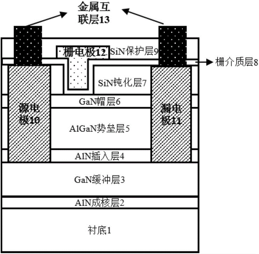
[0032] Embodiment 1, making an AlN dielectric insertion layer 81 with a thickness of 2nm on a sapphire substrate, HfO 2 A GaN-based insulated gate high electron mobility transistor with a high-k dielectric layer 82 having a thickness of 8 nm.
[0033] In step 1, the source electrode 10 and the drain electrode 11 are fabricated on the GaN buffer layer 3 of the epitaxial substrate.
[0034] 1a) Photoetching the region of the source electrode 10 and the region of the drain electrode 11 on the GaN cap layer 6:
[0035] First, bake the epitaxial substrate on a hot plate at 200°C for 5 minutes;
[0036] Then, apply and spin the peeling glue on the GaN cap layer 6, the thickness of the peeling glue is 0.35 μm, and bake the sample on a hot plate at 200°C for 5 minutes;
[0037] Next, apply and spin the photoresist on the stripping adhesive, the thickness of the coating is 0.77 μm, and bake the sample on a hot plate at 90°C for 1 min;
[0038] Afterwards, put the sample that has bee...
Embodiment 2
[0118] Embodiment 2, making an AlN dielectric insertion layer 81 with a thickness of 1 nm on a SiC substrate, Al 2 o 3 The dielectric layer 82 is a GaN-based insulated gate high electron mobility transistor with a thickness of 4nm.
[0119] In step one, the source electrode 10 and the drain electrode 11 are fabricated on the GaN buffer layer 3 of the epitaxial substrate.
[0120] 1.1) Photoetching the region of the source electrode 10 and the region of the drain electrode 11 on the GaN cap layer 6:
[0121] The concrete realization of this step is identical with the step 1a) among the embodiment one;
[0122] 1.2) Evaporate the source electrode 10 and the drain electrode 11 on the GaN cap layer 6 in the region of the source electrode 10 and the region of the drain electrode 11 and on the photoresist outside the region of the source electrode 10 and the region of the drain electrode 11:
[0123] The concrete realization of this step is identical with the step 1b) among the e...
Embodiment 3
[0151] Embodiment 3, making an AlN dielectric insertion layer 81 with a thickness of 1.5nm on a Si substrate, HfO 2 A GaN-based insulated gate high electron mobility transistor with a high-k dielectric layer 82 having a thickness of 6 nm.
[0152] In step A, the source electrode 10 and the drain electrode 11 are formed on the GaN buffer layer 3 of the epitaxial substrate.
[0153] The specific implementation of this step is the same as step 1 in the first embodiment.
[0154] Step B, photoetching the electrical isolation region of the active region on the GaN cap layer 6 , and using an ion implantation process to fabricate the electrical isolation of the active region of the device.
[0155] The specific implementation of this step is the same as step 2 in the second embodiment.
[0156] In step C, a SiN passivation layer 7 is grown on the source electrode 10 , the drain electrode 11 and the GaN cap layer 6 in the active region by PECVD.
[0157] The specific implementation...
PUM
| Property | Measurement | Unit |
|---|---|---|
| Thickness | aaaaa | aaaaa |
| Thickness | aaaaa | aaaaa |
| Thickness | aaaaa | aaaaa |
Abstract
Description
Claims
Application Information