Method for improving properties of non-volatile floating-gate organic thin film transistor type memorizer

An organic thin film and transistor technology, which is applied in the field of organic photoelectric materials, can solve the problems of poor retention characteristics and small memory windows, and achieve the effects of enhancing the ability to capture charges, improving performance, and strong charge-capturing capabilities

Inactive Publication Date: 2017-01-04
FUZHOU UNIV
View PDF2 Cites 7 Cited by
  • Summary
  • Abstract
  • Description
  • Claims
  • Application Information

AI Technical Summary

Problems solved by technology

However, the memory window of the current non-volatile floating gate organic thin film transistor memory is generally small, and the retention characteristics are not very good, which is the most urgent problem to be solved at present.

Method used


Image

  • Method for improving properties of non-volatile floating-gate organic thin film transistor type memorizer
  • Method for improving properties of non-volatile floating-gate organic thin film transistor type memorizer
  • Method for improving properties of non-volatile floating-gate organic thin film transistor type memorizer

Examples


Embodiment 1

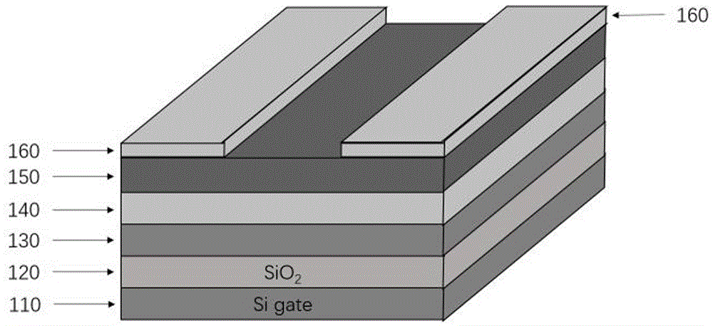
[0044] 1) A heavily doped P-type silicon wafer with a size of about 1.5cm×2.0cm grown with silicon dioxide with a thickness of 100nm is used as a substrate after cleaning with acetone, isopropanol, chloroform, deionized water, etc. and drying with nitrogen.

[0045] 2) Dissolve the organic insulating polymer PVP in a propylene glycol methyl ether acetate solvent at a ratio of 15 mg / ml, and stir at normal temperature for 48 hours to completely dissolve it. This solution was used as the charge storage layer material, filtered with a filter plug, and spin-coated on the silicon wafer substrate obtained in step 1). The spin coating speed is firstly low speed 600rpm / min, time is 5s, and then high speed 2000rpm / min, time is 30s. After spin coating, it was annealed in a glove box for 2 h.

[0046] 3) A layer of aluminum oxide film with a thickness of 4 nm is deposited on the silicon wafer obtained in step 2) by means of atomic layer deposition.

[0047] 4) Dissolve the semiconductin...

Embodiment 2

[0050] 1) A heavily doped P-type silicon wafer with a size of about 1.5cm×2.0cm grown with silicon dioxide with a thickness of 100nm is used as a substrate after cleaning with acetone, isopropanol, chloroform, deionized water, etc. and drying with nitrogen.

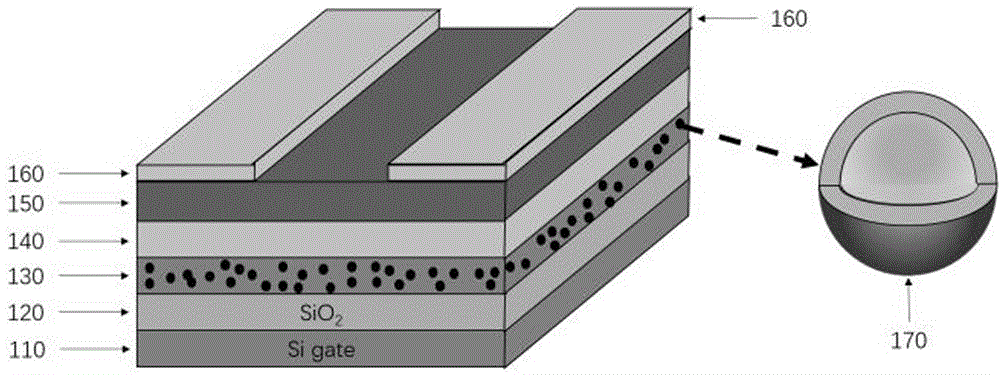
[0051] 2) Dissolve the organic insulating polymer PVP in the propylene glycol methyl ether acetate solvent at a ratio of 15mg / ml, and stir it at room temperature for 48 hours to make it completely dissolved, and dissolve the CdSe / ZnS quantum dots at a ratio of 3mg / ml. Dissolve in chloroform, and then mix the completely dissolved PVP solution and quantum dot solution in a volume ratio of 5:2. This mixed solution is used as the charge storage layer material, filtered with a filter plug, and spin-coated on the silicon wafer substrate obtained in step 1). The spin coating speed is firstly low speed 600rpm / min, time is 5s, and then high speed 2000rpm / min, time is 30s. After spin coating, it was annealed in a glove box for 2 h...


PUM


Abstract

The invention relates to a method for improving properties of a non-volatile floating-gate organic thin film transistor type memorizer, and provides a non-volatile floating-gate organic thin film transistor type memorizer with a bottom-gate top contact structure. According to the non-volatile floating-gate organic thin film transistor type memorizer with the bottom-gate top contact structure, a charge storage layer adopts an organic insulation polymer film doped with quantum dot material; the quantum dot material is of a core-shell structure, and the highest occupied molecular orbital of the nuclear material is higher than that of a shell material, the lowest unoccupied molecular orbital of the nuclear material is lower than that of the shell material, a quantum well is formed between the nuclear material and the shell material, so that the captured electric charges are limited in the nuclear material, the electric charge capture ability of the charge storage layer is improved, and then the memory window of the non-volatile floating-gate organic thin film transistor type memorizer is increased, retention characteristics thereof are significantly improved. The provided method is simple, easy to operate, low in invested cost and enhances the memory property of the memorizer.

Description

technical field [0001] The invention relates to the field of organic optoelectronic materials, in particular to a method for improving the performance of a nonvolatile floating gate organic thin film transistor type memory. Background technique [0002] Non-volatile floating gate organic thin film transistor memory is a kind of transistor memory. Compared with other types of transistor memory, nonvolatile floating gate organic thin film transistor memory has a more complete working mechanism and stronger storage capacity. ability and more stable hold characteristics. The basic principle of nonvolatile floating gate organic thin film transistor memory is to use an external gate voltage to drive the carriers in the organic semiconductor to tunnel into the charge storage layer and be trapped by the charge storage layer, resulting in a shift in threshold voltage. After applying positive (write) and negative (erase) gate voltages respectively, the difference between the threshol...

Claims


Application Information

Patent Timeline
Patent Type & Authority Applications(China)
IPC IPC(8): H01L51/05H01L51/40
CPCH10K10/478
Inventor 陈惠鹏郭太良胡道兵张国成
Owner FUZHOU UNIV
Why Eureka
Try Eureka