Vertical structured chip having multiple color blocks independently emitting light and manufacturing method thereof
A vertical structure and independent light-emitting technology, which is applied in the direction of electrical components, electrical solid devices, circuits, etc., can solve the problems of large pixel dot matrix spacing, large volume, and dazzling LED display images, and achieve the reduction of lamp bead packaging volume, The effects of increased dot matrix density and simplified packaging process
- Summary
- Abstract
- Description
- Claims
- Application Information
AI Technical Summary
Problems solved by technology
Method used
Image

Examples
Embodiment 1
[0028] Fig. 2 shows the implementation steps of the present invention for preparing a vertically structured single-core multi-color block light-emitting chip.
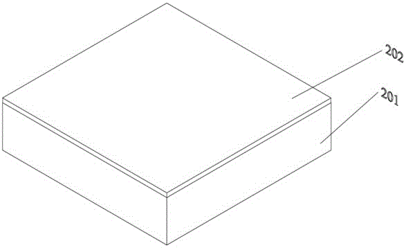
[0029] First, if Figure 2A As shown, the InGaAlN semiconductor light-emitting film 202 is deposited on the epitaxial substrate 201 by metal organic vapor phase epitaxy (MOCVD), and the epitaxial wafer is annealed to activate the P-type layer of the epitaxial film, and vacuum evaporated P Type ohmic cleaning and drying treatment before contacting the reflective metal layer. The method and technology of epitaxial thin film on the epitaxial substrate is a disclosed technology, and the epitaxial substrate 201 can be a sapphire substrate, a silicon carbide substrate, a gallium arsenide substrate or a silicon substrate, or it can be a disclosed pattern Substrates and Composite Substrates.
[0030] Then, if Figure 2B As shown, the P-type ohmic contact metal reflective layer 203 is vacuum evaporated on the InGaAlN semicon...
Embodiment 2
[0045] Figure 3A to Figure 3E A step diagram of another implementation method for preparing a vertical structure single-core multi-color block LED chip according to the present invention is given.
[0046] First formed on the vertical structure wafer as Figure 3A As shown in the photoresist pattern, there is an InGaAlN block 304 exposed except for the electrode pad 305 covered by the photoresist column 306, and the photoresist layer 307 covers the remaining InGaAlN thin film regions In the figure, 302 is the supporting substrate of the wafer, 301 is the metal on the back side of the substrate, and 303 is the metal layer after bonding eutectic. The specific requirements of each structural element in the figure are consistent with the corresponding requirements in Embodiment 1.
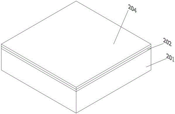
[0047] Then spin-coat and deposit the fluorescent adhesive layer on the wafer, and perform mechanical grinding, thinning, polishing and planarization treatment, such as Figure 3B As shown, 308 is ...
Embodiment 3
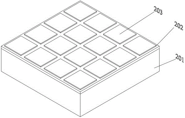
[0050] Figure 4 It is a schematic diagram of a single-core three-color block chip obtained in another embodiment of the present invention. First, the first photolithography process is carried out on the wafer to expose a block of InGaAlN thin film block, and then it is spin-coated with fluorescent glue, centrifugally precipitated and degassed, and then undergoes thermal curing and subsequent mechanical Grinding, thinning and planarization, and selectively removing the photoresist once, so as to obtain the first color block 403 . Then carry out secondary photolithography, spin-coat and solidify the phosphor powder of the second color, thin and planarize through mechanical polishing, and after selectively removing the photoresist, form the second color block 406 on the second block . When the light of the third color is electroluminescent by the InGaAlN thin film 405, it emits blue light of its natural color. 401 in the figure is the supporting substrate of the chip, and 402...
PUM
| Property | Measurement | Unit |
|---|---|---|
| Thickness | aaaaa | aaaaa |
| Thickness | aaaaa | aaaaa |
| Thickness | aaaaa | aaaaa |
Abstract
Description
Claims
Application Information
 - R&D Engineer
- R&D Manager
- IP Professional
- Industry Leading Data Capabilities
- Powerful AI technology
- Patent DNA Extraction
Browse by: Latest US Patents, China's latest patents, Technical Efficacy Thesaurus, Application Domain, Technology Topic.
© 2024 PatSnap. All rights reserved.Legal|Privacy policy|Modern Slavery Act Transparency Statement|Sitemap