Trench field effect transistor and manufacturing method thereof

A field-effect transistor and manufacturing method technology, applied in semiconductor/solid-state device manufacturing, semiconductor devices, electrical components, etc., can solve problems such as device performance degradation and switching speed reduction, and achieve enhanced current density, increased turn-on speed, and improved switching. effect of speed

Active Publication Date: 2017-04-26
芯长征微电子制造(山东)有限公司
View PDF5 Cites 2 Cited by
  • Summary
  • Abstract
  • Description
  • Claims
  • Application Information

AI Technical Summary

Problems solved by technology

[0004] In the conventional structure of Trench MOSFET in the prior art, the thickness of the gate oxide layer at the bottom of the trench is the same as the thickness of the gate oxide layer at other positions, which is relatively thin, resulting in a large gate-drain parasitic capacitance, which reduces the switching speed and reduces the device performance.

Method used


Image

  • Trench field effect transistor and manufacturing method thereof
  • Trench field effect transistor and manufacturing method thereof
  • Trench field effect transistor and manufacturing method thereof

Examples


no. 1 example

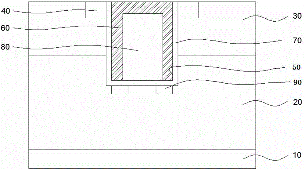
[0035] Such as figure 1 As shown, the trench field effect transistor of this embodiment includes a substrate 10, an n- epitaxial layer 20 formed on the surface of the substrate 10, a p-type body region 30 formed on the surface of the n-epitaxial layer 20, The top of the p-type body region 30 is provided with an n+ active region 40, and the trench 50 extends through the n+ active region 40 and the p-type body region 30 until the n- epitaxial layer 20, and the trench 50 has A polysilicon gate 60 and a gate oxide layer 70, the gate oxide layer 70 is formed on the surface of the trench 50, and the trench 50 also includes an insulating dielectric layer 80 with a dielectric constant not greater than that of the gate oxide layer 70, and the insulating dielectric layer The layer 80 divides the side of the polysilicon gate 60 close to the bottom of the trench 50 into two parts that are respectively close to the p-type body region 30 on both sides, and the bottom of the trench 50 corres...

no. 2 example

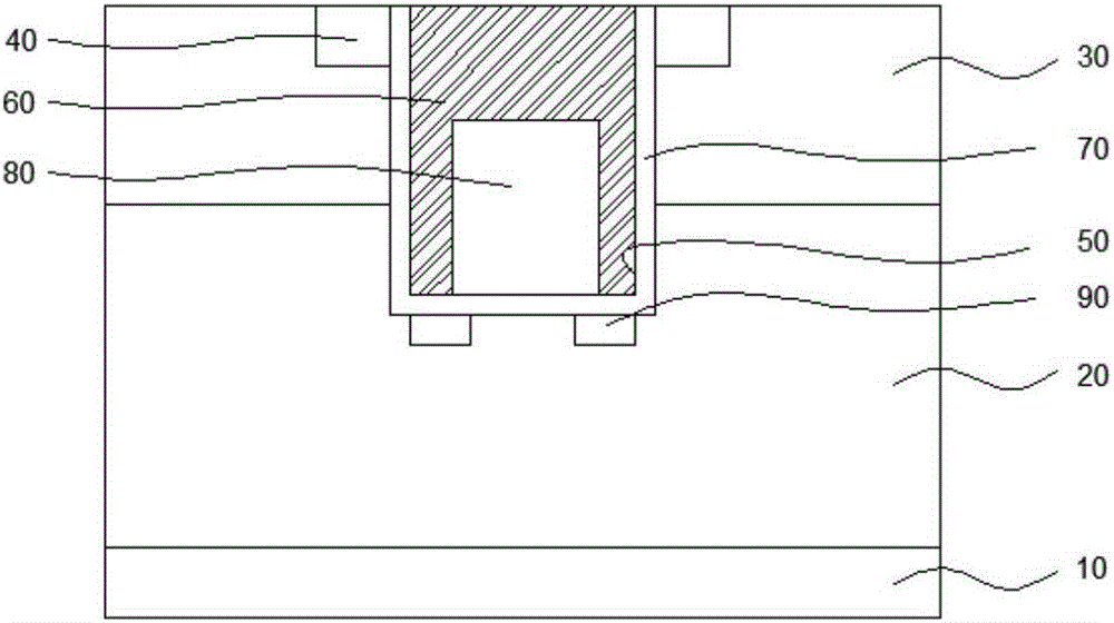
[0049] Such as figure 2 As shown, in the second embodiment, compared with the first embodiment, the distance from the top of the insulating dielectric layer 80 to the bottom of the trench 50 is greater than the distance from the bottom of the n+ active region 40 to the bottom of the trench 50, so that the entire p-type body region 30 corresponds to The current density of the polysilicon gate 60 is uniformly enhanced, which better increases the turn-on speed.

no. 3 example

[0051] Such as image 3 As shown, compared with the first embodiment, the p-type doped region 90 is continuously formed at the bottom of the trench 50 in the third embodiment, which increases the resistance to the high voltage of the polysilicon gate 60 and can simplify doping to form p The process of the type doped region 90.


PUM


Abstract

The invention relates to the technical field of semiconductors, particularly to a trench field effect transistor and manufacturing method thereof. The trench field effect transistor manufactured by the invention includes a substrate, an n- epitaxial layer, a p type body region, n+ active regions, a trench and a polycrystalline silicon gate and a gate oxide layer which are arranged in the trench, the trench also contains an insulating medium layer, the insulating medium layer segments one side of the polycrystalline silicon gate which is close to the bottom of the trench into two parts which are close to the p type body region at two sides separately, and a p type doping region is formed between the trench bottom corresponding to one side of the polycrystalline silicon gate close to the trench bottom and the n- epitaxial layer. The trench field effect transistor provided by the invention effectively reduces gate-drain parasitic capacitance, and improves switching speed.

Description

technical field [0001] The invention relates to the technical field of semiconductors, in particular to a trench type field effect transistor and a manufacturing method thereof. [0002] technical background [0003] Trench MOSFET is a new power device developed rapidly in recent years. Trench MOSFET has high input impedance, low drive current, no minority carrier effect, fast switching speed, high operating frequency, strong current self-regulation ability, uniform current distribution, easy to increase current capacity through parallel connection, and has strong power handling capability. Good thermal stability, large safe working area, no secondary breakdown and other excellent features, have been widely used in various electronic equipment, such as high-speed switching circuits, switching power supplies, uninterruptible power supplies, high-power amplifier circuits, high-fidelity audio circuits , RF power amplifier circuit, power conversion circuit, motor frequency conve...

Claims


Application Information

Patent Timeline
IPC IPC(8): H01L29/423H01L29/78H01L29/06H01L21/336
CPCH01L29/0603H01L29/0684H01L29/4236H01L29/66477H01L29/78
Inventor 李风浪李舒歆
Owner 芯长征微电子制造(山东)有限公司
Why Eureka
Try Eureka