Micro-nano structure interface induced growth method for perovskite film of solar cell

A technology of solar cells and micro-nano structures, applied in nanotechnology, circuits, nanotechnology, etc. for materials and surface science, can solve the problem that metal halides cannot be quickly and completely transformed, and avoid self-organized growth, The effect of shortening the conversion time and increasing the rate

Inactive Publication Date: 2017-05-03
TAIYUAN UNIV OF TECH
View PDF5 Cites 21 Cited by
  • Summary
  • Abstract
  • Description
  • Claims
  • Application Information

AI Technical Summary

Problems solved by technology

[0005] In order to solve the problem that metal halides cannot be quickly and completely converted into perovskite with high phase purity and high uniform morphology in the preparation process of current planar heterojunction and double-layer mesoporous heterojunction perovskite cells, the invention provides a solar energy-oriented Micro-nanostructure interface-induced growth method for high-quality organometal halide perovskite thin films for battery applications

Method used


Image

  • Micro-nano structure interface induced growth method for perovskite film of solar cell
  • Micro-nano structure interface induced growth method for perovskite film of solar cell
  • Micro-nano structure interface induced growth method for perovskite film of solar cell

Examples


Embodiment 1

[0032] Embodiment 1 Utilizes the micro-nano structure interface induced growth method of the perovskite thin film for solar cells of the present invention to prepare an upright planar structure perovskite solar cell:

[0033] 1) Substrate cleaning and preparation of dense electron transport layer: Ultrasonic cleaning of indium tin oxide (FTO) conductive glass with decontamination solution, deionized water, acetone and ethanol for 20 minutes, drying with nitrogen gun, and then UV ozone treatment for 15 minutes to obtain Clean FTO substrate. Then spin-coat 0.15M and 0.3M n-butanol solutions of bis(acetylacetonato)diisopropyl titanate (TiAcAc) on the substrate respectively. After each layer is spin-coated, the substrate is annealed at 125°C for 10min to make the thickness A dense layer of titanium dioxide of about 50 nm;

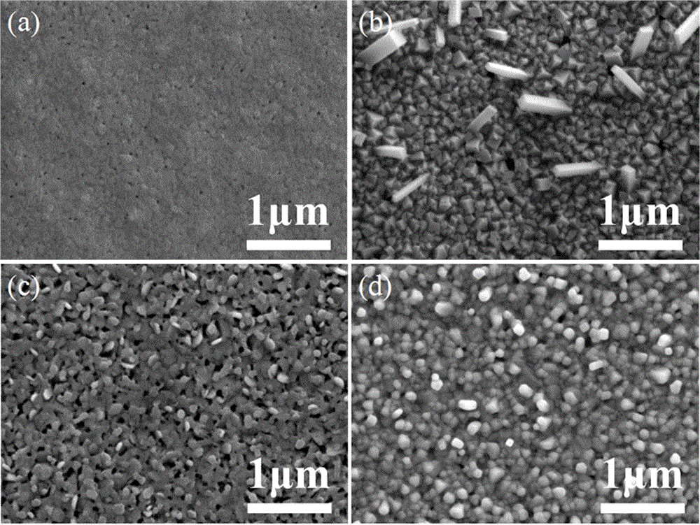
[0034] 2) Preparation of perovskite thin film: 507mg PbI 2 Dissolve in 1mL dimethylformamide, add 78mg dimethyl sulfoxide, and stir at 60°C for 12 hours to o...

Embodiment 2

[0036] Embodiment 2, using the micro-nano structure interface induced growth method of the perovskite film for solar cells of the present invention to prepare upright mesoporous structure perovskite solar cells:

[0037] 1) Substrate cleaning and preparation of dense electron transport layer: Ultrasonic cleaning of indium tin oxide (FTO) conductive glass with decontamination solution, deionized water, acetone and ethanol for 20 minutes, drying with nitrogen gun, and then UV ozone treatment for 15 minutes to obtain Clean FTO substrate. Then spin-coat 0.15M and 0.3M n-butanol solutions of bis(acetylacetonato)diisopropyl titanate (TiAcAc) on the substrate respectively. After each layer is spin-coated, the substrate is annealed at 125°C for 10min to make the thickness A dense layer of titanium dioxide of about 50 nm;

[0038] 2) Preparation of the mesoporous structure electron transport layer: configure the ethanol solution of titanium dioxide nanoparticles (18NRT) with a mass ra...


PUM


Abstract

The invention discloses a micro-nano structure interface induced growth method for an organic metal halide perovskite film of a solar cell, and the method is characterized in that the a solvent coordination-anti-solvent extraction method is employed for preparing a metal halide film with a micro-nano structure interface, and then the micro-nano structure interface is used for inducing the quick conversion and growth of perovskite crystal particles, so as to prepare a high-quality perovskite film and a high-performance solar cell. According to the invention, the coordination solvent in the solvent coordination-anti-solvent extraction method has the strong coordination capability for metal halide, so the crystallization velocity can be reduced. The anti-solvent extraction can avoid the self-organization growth, and achieves the quick deposition to form the film with the micro-nano structure interface, thereby greatly improving the reaction rate of diffusion of organic halide molecules to the interior, and achieving the quick and complete conversion of perovskite. The method does not need to carry out the high-temperature annealing and the vacuum technology, and facilitates the reduction of manufacturing cost.

Description

technical field [0001] The invention belongs to the field of optoelectronic materials and devices, and specifically relates to a method for inducing rapid growth of a high-phase-purity, high-crystal-quality organometallic halide perovskite thin film using a micro-nano structure interface. Background technique [0002] Since organometallic halide perovskite materials were applied to solar cells as a light absorbing layer in 2009, the world record of energy conversion efficiency of perovskite cells has rapidly increased from 3.8% to over 20%. exhibit great application potential. Such a rapid performance improvement is fundamentally due to the excellent photoelectric properties of organometallic halide perovskite materials, such as direct bandgap structure, large optical absorption coefficient, high carrier mobility and large diffusion length. However, the growth of high-quality perovskite films characterized by high phase purity, high crystallinity, uniform morphology, and hi...

Claims


Application Information

Patent Timeline
Patent Type & Authority Applications(China)
IPC IPC(8): H01L51/48B82Y30/00
CPCB82Y30/00H10K71/12H10K71/40Y02E10/549
Inventor 翟光美张继涛高文辉张彩峰邵智猛梅伏洪张建兵杨永珍刘旭光许并社
Owner TAIYUAN UNIV OF TECH
Why Eureka
Try Eureka