
III-nitride semiconductor avalanche photodetector

A nitride semiconductor, avalanche photoelectric technology, applied in the field of detectors, can solve the problems of reducing the filling factor of the device and the difficulty of the manufacturing process, and achieve the effects of reducing surface leakage current, preventing edge breakdown, and high photoelectric gain

Inactive Publication Date: 2017-05-24
江苏华功第三代半导体产业技术研究院有限公司
View PDF5 Cites 12 Cited by
  • Summary
  • Abstract
  • Description
  • Claims
  • Application Information

AI Technical Summary

Problems solved by technology

In other words, the method of tilting the mesa structure also has the disadvantages of difficult manufacturing process and reduced device fill factor.

Method used


Image

  • III-nitride semiconductor avalanche photodetector
  • III-nitride semiconductor avalanche photodetector

Examples


Embodiment Construction

[0021] The present invention will be described in detail below in conjunction with the accompanying drawings.

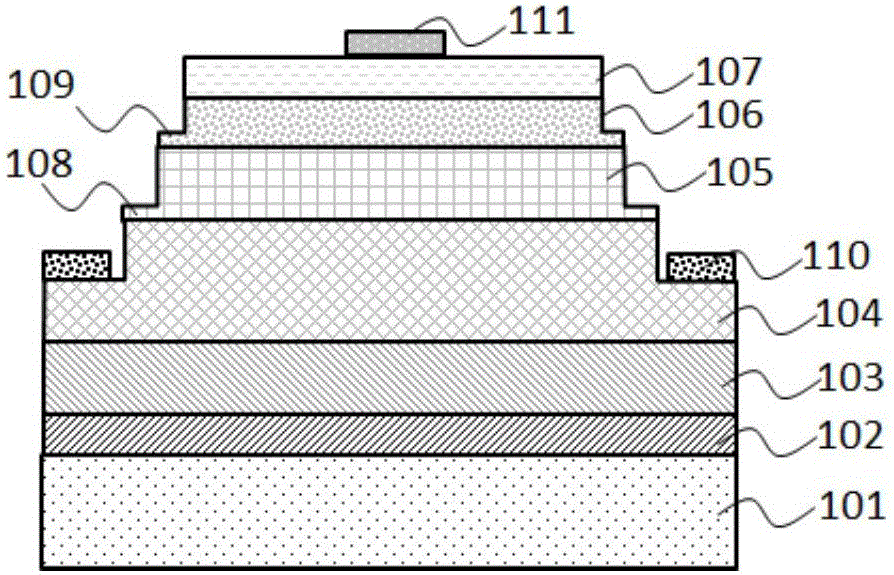
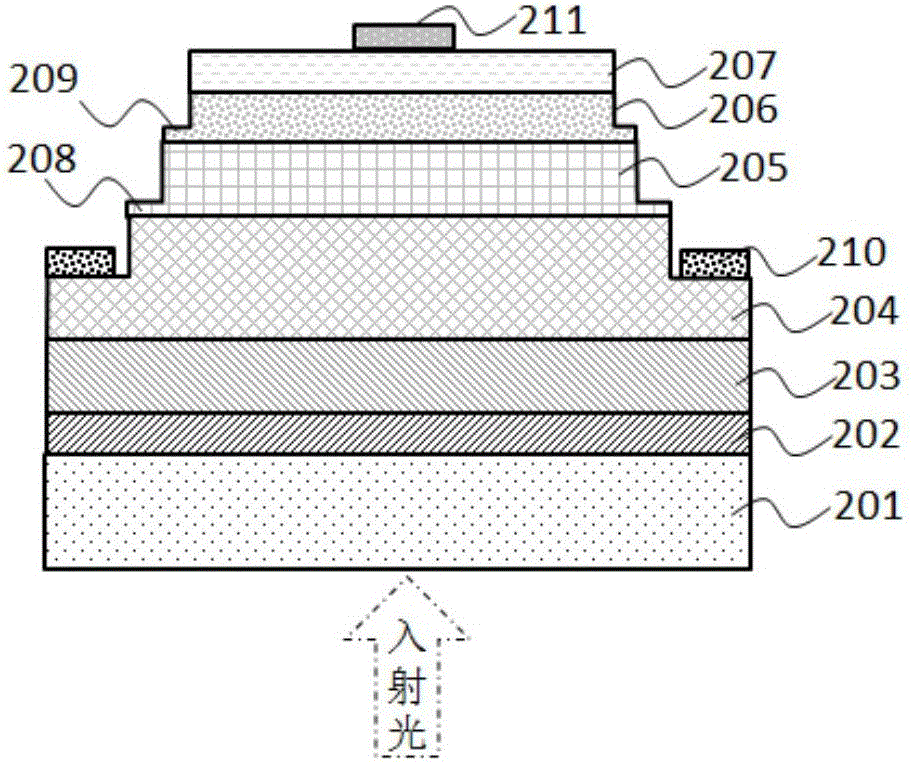
[0022] This example figure 2, a group III nitride AlGaN-based avalanche photodetector is shown in the figure. The device adopts the method of incident light signal from the substrate side, including: a sapphire substrate 201 and a low-temperature AlN buffer layer grown sequentially on the substrate. 202, high temperature AlN transition layer 203, heavily doped n-type Al 0.55 Ga 0.45 N ohmic contact layer 204, non-uniformly doped with p-type Al 0.4 Ga 0.6 N active layer 205, p-type doped Al 0.4 Ga 0.6 N layer 206, heavily doped with p-type Al 0.4 Ga 0.6 N ohmic electrode contact layer 207, the step 208 on the edge of the active layer 205 formed by etching, the step 209 on the edge of the p-type doped layer 206 formed by etching, and the step 209 formed on the n-type Al 0.4 Ga 0.6 The ohmic contact electrode 210 on the N layer 204 is made of p-type Al 0.4 Ga...


PUM

PropertyMeasurementUnit
Thicknessaaaaaaaaaa
Thicknessaaaaaaaaaa
Thicknessaaaaaaaaaa

Abstract

The invention discloses an III-nitride semiconductor avalanche photodetector which comprises a substrate and an epitaxial layer that grows above the substrate. According to a sequence from bottom to top, the epitaxial layer is successively provided with an unintentional adulteration nitride buffer layer, an unintentional adulteration nitride transition layer, a heavy adulteration n-type nitride ohmic electrode contact layer, a heterogeneous light adulteration p-type nitride active layer, a p-type adulteration nitride layer and a heavy adulteration p-type nitride ohmic electrode contact layer. Simultaneously, the invention discloses a device manufacturing method, the method comprises the steps of taking advantage of multiple times of photoetching and dry etching to make steps on the periphery of a device, respectively carrying out vapor deposition of p-type and n-type metal electrodes on the p-type ohmic contact layer and the n-type ohmic contact layer, and forming ohmic contact with a semiconductor through an alloy. According to the device structure, the electric field intensity of an avalanche photodiode active area can be enhanced, and the properties of low dark current, high gain and high detection responsivity of the nitride avalanche photodetector can be realized by effectively increasing the field intensity of the active area and reducing the marginal leakage current of the device.

Description

technical field [0001] The invention relates to a detector, in particular to a low-current, avalanche photodetector based on Group III nitride semiconductor materials and a preparation method thereof. [0002] technical background [0003] With the rapid development of information technology, semiconductor-based solid-state photodetection technology plays an increasingly important role in the field of modern photoelectric information detection. Group III nitride semiconductors represented by GaN-based materials (including their binary compounds GaN, InN, and AlN, ternary compounds InGaN, AlGaN, and AlInN, and quaternary compounds AlInGaN) have wide band gap adjustment ranges, direct band gaps, High electron mobility, high breakdown electric field, high electron saturation drift velocity, high thermal conductivity, small dielectric constant, high temperature resistance, strong radiation resistance, high chemical stability, etc., can be adjusted by ternary or quaternary The co...

Claims


Application Information

Patent Timeline
IPC IPC(8): H01L31/0352H01L31/107H01L31/18
CPCH01L31/0352H01L31/035281H01L31/107H01L31/1848H01L31/1852
Inventor 江灏罗睿宏李顺峰
Owner 江苏华功第三代半导体产业技术研究院有限公司
Learn More