Back-surface tunnel oxidation and passivation inter-digitated type back-to-back contact battery production method

A technology of back-contact battery and tunnel oxidation, which is used in circuits, electrical components, and final product manufacturing, etc., can solve problems such as the need to improve the electrical performance of solar cells, reduce metal-semiconductor surface recombination, improve electrical performance parameters, and change the interface. quality effect

Inactive Publication Date: 2017-05-31
SHANGHAI SHENZHOU NEW ENERGY DEV
View PDF11 Cites 4 Cited by
  • Summary
  • Abstract
  • Description
  • Claims
  • Application Information

AI Technical Summary

Problems solved by technology

However, this kind of solar cell still has the problem

Method used


Image

  • Back-surface tunnel oxidation and passivation inter-digitated type back-to-back contact battery production method

Examples


Embodiment 1

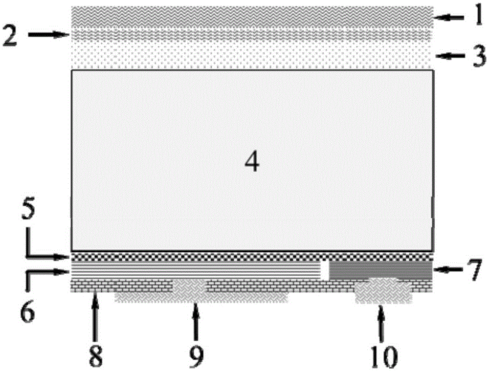
[0026] The fabrication method of back surface tunnel oxidation passivation interdigitated back junction back contact battery adopts the following steps:

[0027] (1) Using the silicon chip in KOH alkali solution and H 2 o 2 Remove the damaged layer in the solution, and then use a mixed solution of tetramethylammonium hydroxide and isopropanol to texture the front side of the silicon wafer to form a pyramid textured surface with a thickness of 1 μm;

[0028] (2) Diffusion or ion implantation is adopted on the front side of the silicon wafer to form N + front surface field;

[0029] (3) Use HF solution to remove the PSG layer of phosphosilicate glass, and use HNO 3 Mixed solution with HF for side insulation and back polishing;

[0030] (4) Using wet chemical method or dry thermal oxidation method to grow an ultra-thin tunnel oxide layer SiO on the back of the silicon wafer 2 , in this example, fluosilicic acid H 2 SiO 6 solution, the concentration is 1.3M, protect the fro...

Embodiment 2

[0038] The fabrication method of back surface tunnel oxidation passivation interdigitated back junction back contact battery adopts the following steps:

[0039] (1) Using the silicon chip in NaOH alkali solution and H2 o 2 Remove the damaged layer in the solution, and then use a mixed solution of tetramethylammonium hydroxide and isopropanol to texture the front side of the silicon wafer to form a pyramid textured surface with a thickness of 2 μm;

[0040] (2) Diffusion or ion implantation is adopted on the front side of the silicon wafer to form N + front surface field;

[0041] (3) Use HF solution to remove the PSG layer of phosphosilicate glass, and use HNO 3 Mixed solution with HF for side insulation and back polishing;

[0042] (4) Using wet chemical method or dry thermal oxidation method to grow an ultra-thin tunnel oxide layer SiO on the back of the silicon wafer 2 , in this example, fluosilicic acid H 2 SiO 6 solution, the concentration is 1.5M, protect the fron...

Embodiment 3

[0049] The fabrication method of back surface tunnel oxidation passivation interdigitated back junction back contact battery adopts the following steps:

[0050] (1) Using the silicon chip in KOH alkali solution and H 2 o 2 Remove the damaged layer in the solution, and then use a mixed solution of tetramethylammonium hydroxide and isopropanol to texture the front side of the silicon wafer to form a pyramid textured surface with a thickness of 4 μm;

[0051] (2) Diffusion or ion implantation is adopted on the front side of the silicon wafer to form N + front surface field;

[0052] (3) Use HF solution to remove the PSG layer of phosphosilicate glass, and use HNO 3 Mixed solution with HF for side insulation and back polishing;

[0053] (4) Using wet chemical method or dry thermal oxidation method to grow an ultra-thin tunnel oxide layer SiO on the back of the silicon wafer 2 , in this example, fluosilicic acid H 2 SiO 6 Solution, the concentration is 1.7M, protect the fro...


PUM

PropertyMeasurementUnit
Thicknessaaaaaaaaaa
Thicknessaaaaaaaaaa
Thicknessaaaaaaaaaa

Abstract

The invention relates to a back-surface tunnel oxidation and passivation inter-digitated type back-to-back contact battery production method, comprising: removing the damage layer of a silicon wafer and making velvets; and then forming an N + front surface field on the front surface of the silicon wafer; removing the phosphor silicate glass (PSG) layer and performing edge insulation and back polishing; growing an ultra-thin tunnel oxide layer SiO2 on the back of the silicon wafer; forming an inter-digitated type polysilicon layer composed of a polysilicon layer of B-doped and P-doped pairs; depositing an aluminum oxide layer and a hydrogenated amorphous silicon nitride passivation antireflective layer on the surface of the N + front surface field; and growing a silicon layer on the back side of the wafer; printing Ag/Al slurry on the back side of the battery corresponding to the B-doped region through the use of the screen printing method; printing the Ag slurry in the P-doped region; and then, drying the slurries in an oven. The invention utilizes an ultra-thin tunnel oxidation SiO2 layer and an interdigitated phosphorous-doped and boron-doped silicon layer, which greatly alters the interface quality of the silicon substrate and greatly reduces the composition of the back surface metal and the semiconductor surface.

Description

technical field [0001] The invention relates to a manufacturing method of a crystalline silicon battery, in particular to a manufacturing method of a back surface tunnel oxidation passivation interdigitated back junction back contact battery. Background technique [0002] Solar cells are currently widely used products, and Chinese patent CN102800716A discloses a solar cell and a manufacturing method thereof. The substrate of the solar cell has a heavily doped region and a lightly doped region. Both the anode and the cathode are arranged on the back of the substrate, so the amount of light incident on the front of the substrate can be increased. The anode and the cathode are in contact with the heavily doped region to form a selective emitter structure, thus having a lower contact resistance. In addition, the lightly doped region not in contact with the electrode has a lower saturation current, thus reducing the recombination of electron-hole pairs and increasing the absorp...

Claims


Application Information

Patent Timeline
IPC IPC(8): H01L31/0352H01L31/0224H01L31/18
CPCH01L31/0224H01L31/022441H01L31/0352H01L31/18Y02P70/50
Inventor 汪建强钱峥毅郑飞马贤芳林佳继张忠卫石磊阮忠立
Owner SHANGHAI SHENZHOU NEW ENERGY DEV
Why Eureka
Try Eureka